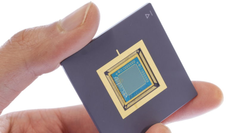
Swiss take in-memory computing 2D
Researchers from EPFL stepped into unexplored territory by creating an in-memory processor based on a 2D material. With in-memory computing already an emerging strategy to cut down on the energy needed for digital signal processing and the implementation of artificial intelligence models, the use of 2D materials could further lower energy bills.
Today’s universally adopted architecture, devised by John von Neumann, spends a lot of energy shuttling data between memory and processor. This physical separation between components that process data and components that store data has long been a necessity, as it simply wasn’t possible to combine both in a single component.
These days, the Von Neumann architecture is being challenged by more efficient alternatives. “There are ongoing efforts to merge storage and processing into more universal in-memory processors that contain elements that work both as a memory and as a transistor,” explains Andras Kis, professor of electrical engineering at EPFL and lead author of the study published in Nature Electronics.
For example, Eindhoven-based Axelera AI recently raised 50 million dollars to take its first-generation AI acceleration product into mass production. This Metis platform is fully CMOS compatible.

Entire wafers
Looking further into the future, Kis’ lab is investigating whether in-memory computing and 2D materials are a good match. Consisting of a few atomic layers at most, electrons travel remarkably easily through this class of materials. This is why they’re being considered as possible successors to silicon as the semiconductor industry’s base material. Molybdenum disulfide (MoS2) and other molybdenum compounds are frontrunners because of their intrinsic band gaps, facilitating switching action.
Back in 2010, the EPFL group was the first to create a MoS2 transistor. The researchers peeled off a monolayer of the material from a crystal using scotch tape, much in the same way as the first graphene transistor was made a few years earlier.
Over the past 13 years, processes to create MoS2 transistors – and integrated circuits - have matured substantially. “The key advance in going from a single transistor to over 1,000 was the quality of the material that we can deposit. After a lot of process optimization, we can now produce entire wafers covered with a homogeneous layer of uniform MoS2. This lets us adopt industry standard tools to design integrated circuits on a computer and translate these designs into physical circuits, opening the door to mass production,” says Kis.
Single step
The new processor combines 1,024 elements onto a one-by-one-centimeter chip, with each element comprising a molybdenum sulfide transistor as well as a floating gate, used to store a charge in its memory that controls the conductivity of each transistor. Coupling processing and memory in this way fundamentally changes how the processor carries out calculations. It’s particularly useful for so-called analog vector-matrix multiplications, operations that are ubiquitous in digital signal processing and the implementation of artificial intelligence models, for example.
“By setting the conductivity of each transistor, we can perform analog vector-matrix multiplication in a single step by applying voltages to our processor and measuring the output,” explains Kis.


