Canon’s nanoimprint announcement: seeing is believing
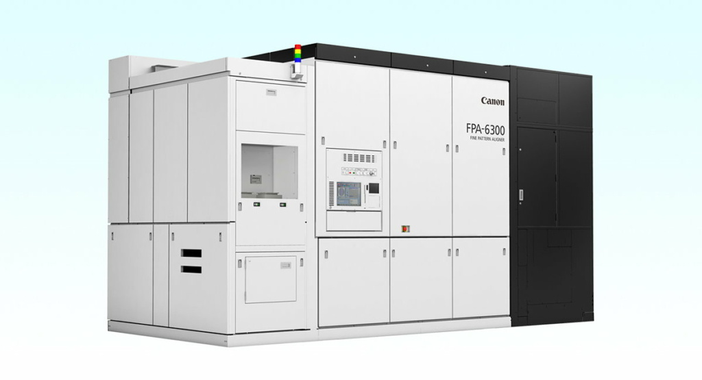
Canon has big plans for nanoimprint lithography (NIL). “By bringing to market semiconductor manufacturing equipment with NIL technology, Canon meets the needs of a wide range of users by covering from the most advanced semiconductor devices to the existing devices,” the company states in a press release, adding that its machine is capable of producing 5nm-node patterns, which will extend to the 2nm node after improvements in mask technology.
Few people believe NIL will be used to manufacture such advanced chips, or even logic chips in general, anytime soon. Even Canon itself acknowledges there are obstacles ahead. “We’re still facing challenges before we can reach the levels required for mass production,” Kazunori Iwamoto, head of Canon’s Semiconductor Production Equipment Group, told Japanese newspaper Asahi Shimbun.
Workhorse
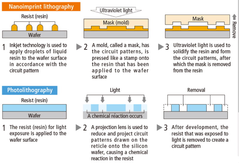
Nanoimprint lithography creates nanometer-scale patterns by pressing a mask into a resin-coated wafer surface and then hardening it using UV light before removing the mask for another round. Just like optical lithography, a wafer is usually processed step-wise, requiring many rounds of ‘stamping’ to cover the entire surface.

NIL has a few things going for it. Compared to optical and especially EUV lithography, the equipment is less complex and the process requires fewer steps. In theory, it can produce smaller structures with smoother edges than EUV lithography. Parallelization of the comparatively slow NIL process and/or increased mask sizes would benefit throughput.
First included in the International Technology Roadmap for Semiconductors in 2003, NIL traditionally has faced a number of challenges. First, even perfect masks don’t necessarily transfer patterns perfectly: air bubbles trapped between resin and mask cause so-called non-fill defects. Shear forces during the separation of the mask and the (hardened) resin as well as stray particles may distort the pattern and contaminate the mask. Second, it has proven notoriously difficult to precisely align one chip layer to the next, causing detrimental errors. And third, NIL needs to show a compelling cost advantage.
Commercialization
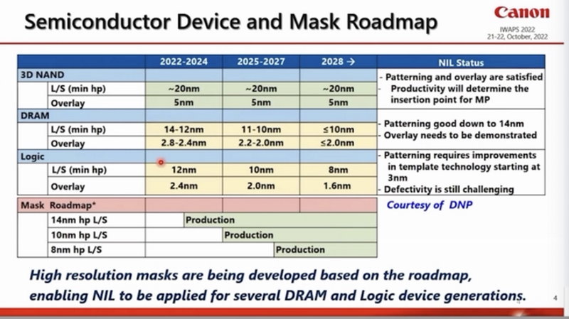
At the recent product announcement, Canon didn’t specify its progress in solving these issues. In a presentation last year, however, it listed productivity as the final hurdle for manufacturing 3D-NAND using NIL. Being an extremely cost-sensitive business and NAND structures being more tolerant to defects and overlay errors, 3D-NAND is quite possibly the best point of entry for NIL into the semiconductor space. DRAM and logic are also included in Canon’s roadmap, although these still face defectivity and overlay issues.

Canon has announced a 350-million-dollar investment in a new lithography equipment manufacturing facility, which will include NIL equipment fabrication. Construction is scheduled to commence next year and finish in 2025, but no company has hinted at adopting NIL in high-volume production in the near future. Both SK Hynix and Kioxia (formerly Toshiba) have been testing Canon’s NIL equipment for a few years now. In May, SK Hynix stated that “there has been no discussion on possible introduction or commercialization of nanoimprint lithography.”
Main picture credit: Canon


