High-NA tee-off has been set: 2026
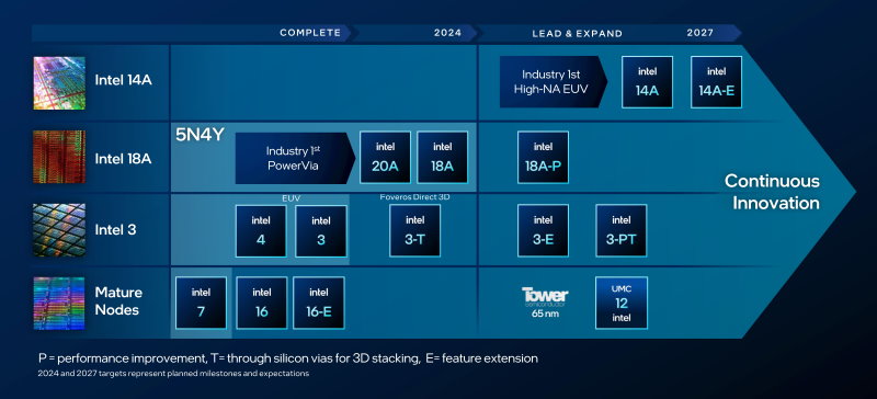
Intel will deploy ASML’s high-NA EUV tools before 2027, the chip company unveiled. Speaking at the firm’s IFS Direct Connect event, CEO Pat Gelsinger confirmed that the upcoming 14A node will make use of high-NA. Although no explicit timing was announced, it’s safe to assume that 14A is scheduled for 2026, given the company’s recent cadence of at least one node per year. Intel said that the preceding 18A node is on track to start high-volume manufacturing in the second half of this year.
The timing matches the prediction of ASML, which said that the industry would see large-scale adoption of high-NA in the 2026/2027 time frame. TSMC and Samsung haven’t announced their plans for the next-generation EUV tool, however. There have been reports that the introduction has been delayed due to cost concerns. ASML has fired back at these allegations, and Intel told Tom’s Hardware that high-NA is cost-effective for the company’s purposes.
Still, Intel’s fast-paced adoption isn’t without risk. The company was very late to the EUV party – its first full-on EUV node (Intel 4) started ramping not so long ago. Several challenges remain to use high-NA effectively in manufacturing, and a relative lack of experience with EUV in general doesn’t help to scale those hurdles. On the other hand, Intel is currently an underdog in the global leading-edge semiconductor landscape and a calculated risk or two may be required to get back on top.
Software giant
At IFS Direct Connect, Intel announced its ambition to become the world’s second-largest foundry by 2030. To this end, the company is essentially splitting in half, creating a foundry and a product business. These entities will be legally distinct and will operate independently from each other, although there will be some interdependence in that Intel Product will be Intel Foundry’s biggest customer for the foreseeable future. The company’s first high-volume 18A CPU called Clearwater Forest was recently taped out.
Intel is making headway in recruiting external customers, though. With several companies getting on board across various processes as well as advanced-packaging services, the order book has now grown to 15 billion dollars. At the event, CEO Satya Nadella announced that Microsoft will be among the fabless companies utilizing the 18A node to manufacture a custom IC. Details about the chip weren’t given, but it’s been reported that the software giant has been working on its own silicon for processing and AI.
Massive flywheel
On top of competitive offerings, Gelsinger is hoping geopolitical anxiety will help lure additional customers to his shop. He said the world’s semiconductor supply chain isn’t “resilient,” with the pandemic and a number of hot and cold conflicts around the globe demonstrating the need for a more sturdy ecosystem. He also promised not to compromise on sustainability and make Intel the world’s most eco-friendly foundry.
An appearance by Commerce Secretary Gina Raimondo served to hammer home the message that reshoring semiconductor manufacturing has the full support of the US government. Raimondo wants to get a “massive flywheel” going on US shores, a “self-propelling engine of innovation and production” from “research all the way to advanced packaging” to recapture leading-edge manufacturing capacity market share in particular.
Intel will likely be a major vehicle for that effort, but Raimondo wasn’t ready to announce concrete support from the coffers of the US Chips and Science Act. It was previously reported that Intel is set to receive 10 billion dollars in subsidies. Three companies – Globalfoundries (1.5 billion dollars), Microchip Technology (162 million dollars) and BAE Systems (35 million dollars) – have already been awarded funding.
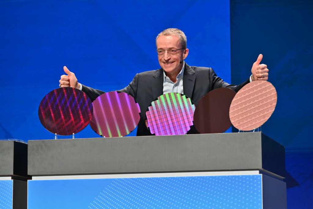
Main picture: Intel CEO Pat Gelsinger with his ‘babies.’ Credit: Intel


