

Bosch’s approach to MEMS using multi-physics simulation
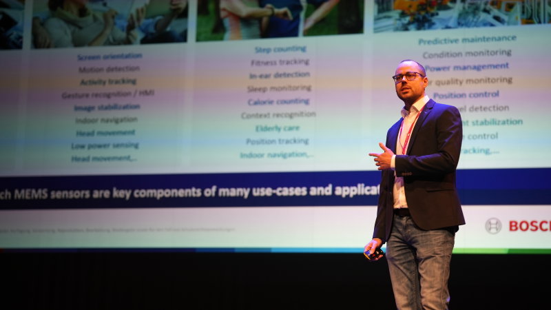
Bosch has been active in MEMS development for roughly three decades. What started in automotive safety applications, such as airbag deployment and electronic stability control, has grown into a broad portfolio spanning consumer electronics, healthcare and industrial systems. In the consumer electronics industry, where motion and environmental sensing play a central role, the German company is one of the major suppliers.
A typical MEMS device combines a microscopic mechanical structure with an application-specific integrated circuit (ASIC), electrical interconnects and protective packaging. Together, these components form a miniature system that translates physical quantities like motion, pressure and magnetic fields into electrical signals. The mechanical structures themselves operate at micrometer scales. In an accelerometer, for example, a tiny mass is suspended by microscopic springs inside a silicon structure. When the device accelerates, the mass moves slightly, changing an electrical property such as capacitance. That change is detected and processed electronically.
At a recent Comsol conference in Amsterdam, keynote speaker Daniel Maier of Bosch offered a rare look into how his company designs and industrializes MEMS sensors and actuators. “A typical membrane of a capacitive pressure sensor may be 300 by 150 micrometers in size,” explained Maier, a senior MEMS designer with over fifteen years of experience in modeling and simulation across various product fields and physical domains. “For a pressure change corresponding to someone climbing one stair, the membrane deflects by about 6 picometers, which is less than atomic scale.”
Automated workflow
MEMS sensors are manufactured at the wafer level. This means that thousands of devices are produced simultaneously. As a result, engineers must account for process tolerances and statistical variations across an entire wafer, not just a single design instance.
At the same time, MEMS devices are inherently multi-physical. A single sensor may involve structural mechanics, electrostatic or piezoresistive effects, heat transfer and fluid dynamics. These coupled effects determine performance, noise levels, sensitivity and long-term reliability.
Bosch’s MEMS development has matured to make high-volume industrialization possible with high yields. The company relies heavily on multi-physics simulation as part of an automated development workflow. Simulation is used to understand individual sensor concepts and to explore design trade-offs, assess robustness and predict yield under manufacturing variations. “There often are multiple requirements that aren’t so easy to meet, so we do multi-objective optimization,” said Maier in his keynote speech.
Because wafer runs are expensive and time-consuming, Bosch emphasizes high prediction reliability early in the design process. Maier: “We put all our models for predicting the sensor behavior into an automated tool chain with a single source approach.”
Iterative refinement
Maier illustrated Bosch’s capabilities with two development examples. One is a MEMS-based microspeaker for true wireless in-ear devices. The concept relies on in-plane mechanical motion on a wafer to generate out-of-plane airflow, producing sound. The model for this system showed a top wafer, a bottom wafer, inlets and outlets, and lamellas that move air from the bottom to the top. Maier went into the multi-physical simulation challenges for this example. “The lamellas have mechanical stiffness. We also have electrostatics to drive the lamellas and we deal with acoustics. Comsol’s acoustic module describes all the microfluidic behavior in the channels and the chamber.”
Another example comes from the automotive domain: a hydrogen gas sensor designed to detect leaks in fuel-cell vehicles. The sensor exploits hydrogen’s high thermal conductivity relative to air. It compares the temperature in the measurement chamber, where hydrogen would flow into in case of a leak, to the temperature of a control chamber without hydrogen, under identical electrical heating. A lower steady-state temperature in the measurement chamber indicates hydrogen presence. By modeling electrical currents and heat transfer together, Bosch can predict temperature distributions, sensor sensitivity and offsets before fabrication.
Bosch’s modeling strategy evolves with sensor maturity. Early-stage concepts may rely on analytical or first-order models with limited predictive accuracy. As development progresses and validation data accumulates, models are refined to capture the relevant physical effects more accurately. For mature sensors, Maier indicated that prediction accuracy can reach the percentage range – sufficient to support confident design decisions at industrial scale. This iterative refinement, grounded in both simulation and measurement, is central to Bosch’s MEMS strategy.
When asked by the audience what kind of machines Bosch uses to run the simulations on, Maier answered: “We use our own high-performance computing systems. However, HPC isn’t always helpful for individual simulations because many models require ramping from previous solutions. Where HPC helps is in running multiple parameter sets in parallel.”


