Your cart is currently empty!

ChipNL kicks off with a design platform for chips
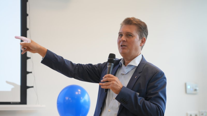
The EU Chips Design Platform aims to lower the threshold for IC designs, particularly for startups and academia. During the launch of ChipNL at the Noviotech Campus in Nijmegen, coordinator Romano Hoofman laid down the broad outlines.
“A very complicated mission.” That’s how Romano Hoofman, coordinator of the EU Chips Design Platform, defines Europe’s attempt to build a cloud-based, distributed infrastructure for IC design. The initiative focuses specifically on startups and small and medium-sized companies.
Hoofman unveiled the structure, goals and rollout of the design platform at the official launch of the ChipNL Competence Center at the Noviotech Campus in Nijmegen. The center, backed by both the European Union and the Dutch Ministry of Economic Affairs, aims to provide a national interface to the broader ambitions of the EU Chips Act.
The context: global demand for semiconductors is expected to double by 2030. Yet, Europe’s share in this rapidly expanding market continues to lag. This vulnerability became painfully visible during the Covid pandemic, when supply disruptions revealed the region’s dependence on foreign technology. It’s now reinforced by the way the United States is disrupting the international order with a winner-takes-all approach.
Romano Hoofman positions the EU Chips Design Platform (EuroCDP) at the core of the Chips for Europe Initiative. “If the European Commission’s vision is to be realized, many technical and operational challenges lie ahead.” The users – fabless startups and SMEs – are the ultimate beneficiaries, Hoofman pointed out. “The design platform will enable design and manufacturing from the pilot lines, but also from commercial foundries like TSMC, Globalfoundries and smaller ones like X-Fab. Product companies really have to make their chip in a very fast way.”
Go-to place
The motivation behind the platform is to democratize access to IC design tools, technologies and services. “We lower the chip design barrier for small companies, startups and SMEs,” Hoofman said. This doesn’t mean that integrated device manufacturers (IDMs) like NXP or others can’t use the design platform. “But for the first years, that’s not the focus,” Hoofman explained. The intention is clear: help small, innovative firms bring products to market faster and keep them within the European ecosystem.
To do so, the platform builds on and expands existing initiatives. The most prominent one is Europractice, an EU program run by Imec that provides access to design tools and multi-project wafer (MPW) services with a strong focus on academia. The EuroCDP initiative goes far beyond that. “The Commission has already called EuroCDP ‘Europractice on steroids,’” Hoofman noted, smilingly. Its goal is to develop a cloud-based infrastructure where you can find everything. Startups will find references to EDA tools, IP blocks, design enablement teams, training programs and paths to production. “You could call it the go-to place for IC design to product.”
The platform consists of several interacting layers. At its heart is a central cloud environment that acts as a marketplace. Hoofman: “There, you can find the enabling design environment offering design IP and also references to EDA. We’re negotiating favorable terms for startups on EDA licenses. Not only will commercial providers be there, you’ll also get access to open-source tooling.”
The process design kits (PDKs) won’t be hosted in the central cloud. They’ll be hosted by design enablement teams. These are physical consortia distributed across Europe, responsible for actual design support, fabrication coordination, packaging, testing and interfacing with foundries. “They’ll support you with the design and access to the PDKs and to the wafer fabs. Because it’s not only the chip design; it’s also the package, the testing. Everything that you need to make a commercial product in the end.”

Structured journey
Located at Imec, Hoofman leads the Platform Coordination Team (PCT), which oversees the platform activities. The PCT is responsible for the overall coordination of the design platform to set up mentoring and training programs for startups, link to the other European chip initiatives and negotiate framework and master agreements with the EDA and IP vendors.
The PCT also coordinates the onboarding of design enablement teams. Nine of these teams have been selected to negotiate grant agreements. One of them, focusing on photonics, is anchored in Eindhoven – a clear recognition of the Netherlands’ strengths in this domain.
A central budget of 220 million euros from the European Commission will be distributed via the PCT to eligible startups. Hoofman: “Typically, early startups will be favored most.” National governments are expected to match this funding. “Suppose a Dutch startup wants to make a design in the Netherlands and they apply for a 10-million-euro budget. It can then get 3.5 million euros from the Commission and through us, 3.5 million euros from the Netherlands and 3 million self-funded. The latter can come from venture capital, a rich uncle or whoever puts the money on the table. This is a considerable package that will boost the startup’s development. The eligible costs are the costs for the EDA, IP, fabrication, testing, design services – everything you need to make your first prototypes.”
The platform also offers a structured startup journey, from orientation to prototyping and upscaling. “We’ll create an open-source sandbox environment to upscale the design skills of startups. We offer training as well, and together with the competence centers, we hope that they can select which technology is best for the applications they have in mind.”
Maturing companies can enter incubation or acceleration programs. “We’ll provide mentoring and classroom training to improve not only their technical skills but also their business skills. To mature their go-to-market plan.”
A key goal is to avoid the need for technology transitions mid-trajectory. “It’s crucial that we get this ramp-up done in a good way. And again, that you don’t need to transition from one technology to another because you can’t scale up. That would really be a waste of time.”
Hoofman categorizes a company as a very early startup if it has gathered up to 1 million euros in capital. “They can get very cheap EDA licenses – maximum 10,000 euros for ten ‘full license suites.’” Larger startups (up to 20 million in gained capital) will also get a good deal. Companies that have more than 20 million aren’t considered a startup anymore by the EDA vendors and need to directly negotiate commercial licenses.
EuroCDP works closely with existing incubators such as Chipstart EU, an initiative of Silicon Catalyst. “We have an agreement that once companies graduate from there, they can also get into our accelerator.”
Milestones
Security was another topic raised by the audience, especially concerning cloud-based design environments and geopolitical dependencies. Hoofman addressed both. “The cloud is a very secure environment where designers can do their work. It’s also to keep, for instance, the PDK secure from TSMC or other foundries.”
As for the question of European-only technology, Hoofman would recommend not only focusing on Europe, “because the market leaders for EDA are Cadence and Synopsys. If you restrict yourself to Europe, you’re limiting the startups’ ability to make progress. We need to work together at least with the like-minded countries. And for me, the US is still like-minded.”
Looking ahead, several milestones are in view. The mini-marketplace will go live in early 2026, offering deals with EDA/IP vendors. The first startup grants are expected to be available in Q2. Full rollout of the central cloud is planned for the end of next year. The first incubation and acceleration programs will start in June 2026, with tailored training materials on business and entrepreneurship in the IC domain.


