As Intel starts assembling its first high-NA EUV scanner, one analyst questions the cost-effectiveness of the next-generation lithography tool for upcoming nodes. TSMC might not be convinced, either.
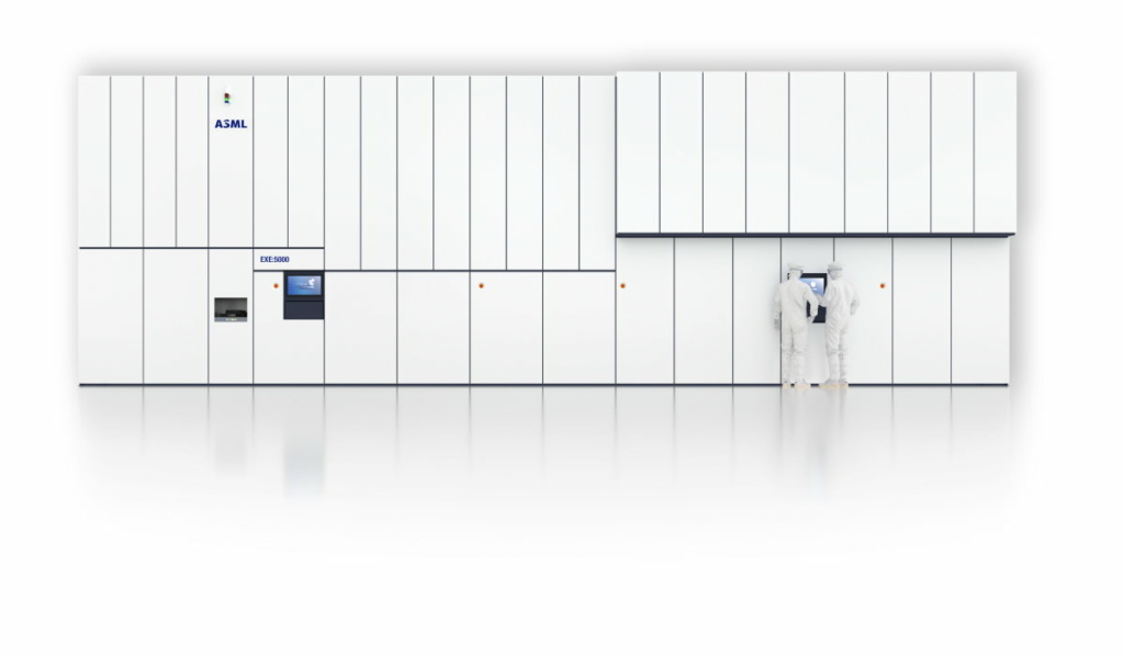
Intel has received the first shipment of high-NA EUV scanner components from ASML at its manufacturing and R&D site in Oregon, the chipmaker announced on X (formerly Twitter). The companies will soon start assembling the next-generation lithography tool, which is intended for process development. Intel will probably announce the timing of high-NA insertion into high-volume manufacturing at its Intel Foundry Services Direct Connect event on 21 February, but it will likely be around the start of 2026 at the earliest, since full-fledged high-NA production systems are expected to start shipping later this year. Reportedly, the American semicon giant will receive six out of the first ten units.
Early adoption of high NA is a key element of Intel’s ambition to regain technological leadership in the semiconductor industry. By contrast, the company was slow to adopt ‘regular’ EUV lithography, starting EUV-enabled mass production in September 2023, roughly four years behind Samsung and TSMC. Struggling with quadruple patterning and unrealistic scaling targets, Intel stumbled. After taking the helm in 2021, CEO Pat Gelsinger vowed to get back on top by delivering five new nodes in four years.