Philips research veteran Fred Roozeboom’s career honored with Gordon E. Moore medal
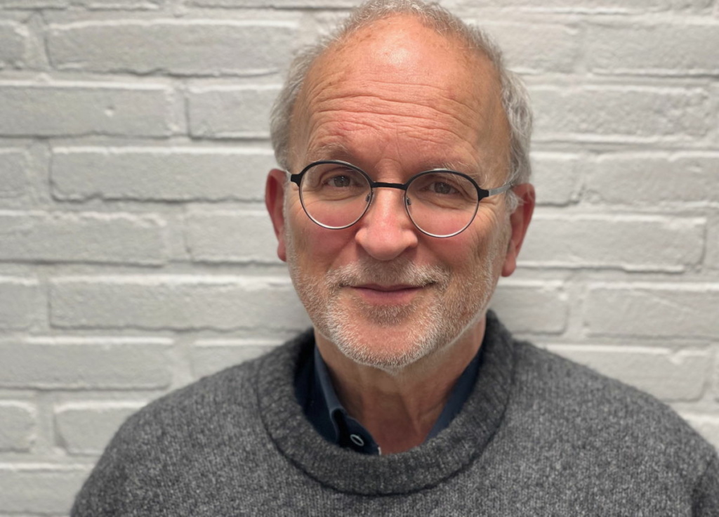
The Electrochemical Society (ECS) has bestowed the Gordon E. Moore Medal for Outstanding Achievement in Solid State Science & Technology to Fred Roozeboom, former research fellow at Philips and NXP. Established in 1971 as the Solid State Science and Technology Award, it was renamed in 2005 to honor the achievements of Gordon Moore in the field of microelectronics. Former recipients include Nobel laureate Isamu Akasaki and solar cell inventor Gerald Pearson. Roozeboom is the first European to receive the prize.
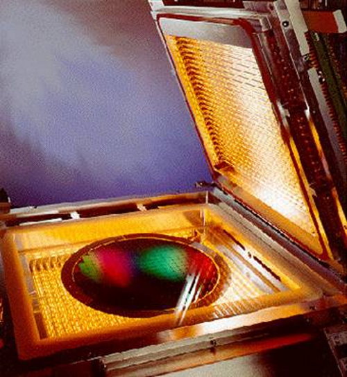
The award salutes lifetime achievements, and Roozeboom’s career can be summarized with only two words: short pulses. His first assignment at Philips Research, which he joined in 1983 after obtaining a PhD degree in inorganic chemistry at the University of Twente, focused on rapid thermal processing (RTP), ie exposing a silicon wafer to a ‘pulse’ of heat. Such a heat treatment, performed on single wafers, alters the physical and chemical properties of materials and is an important tool in the semiconductor processing toolkit.
“At the time, wafers were still annealed in large batch ovens. These have huge heat capacity, meaning it takes a relatively long time to reach the target temperature. This results in unwanted chemical processes. Temperature uniformity while heating across the wafer was an issue, too. As scaling continued and chip structures shrank, these issues were turning into showstoppers,” Roozeboom explains, reminding the interviewer that Philips Research at the time was involved in cutting-edge CMOS development.

“I feel that I made some relevant contributions to the development of RTP for semiconductor manufacturing. I was particularly involved with perfecting in-situ temperature measurements to better understand the physics involved, among other things,” says Roozeboom. His technique of choice, pyrometry, was pioneered by others. It involves temperature measurement by measuring the thermal emission of the wafer. “Definitely not straightforward, considering the nearby heat sources: the lamps used to heat the wafer.”
High aspect
After an intermezzo in magnetic recording heads in the first half of the 90s, Roozeboom returned to semiconductor processing, leading a project to integrate decoupling capacitors into RF chips. Such integration of passive components on chips reduces the number of parts in an electronic system, thus saving in power consumption as well as space. These are important features in space-constrained applications such as mobile phones. Additionally, there are cost benefits.
Roozeboom was particularly focused on 3D passive integration, in which the capacitors and ASICs are stacked on top of each other, saving even more space, to create a system in package (SiP).
“In his original article describing what we now know as his famous law, Gordon Moore noted that integration of passives wasn’t an attractive option because they don’t scale well. In those days, he didn’t fully realize that by going 3D, it is possible to manufacture compact capacitors in silicon.” These capacitors are essentially holes drilled into the wafer, filled with a sandwich of an insulator between two metal layers (metal-insulator-metal or MIM capacitor). Holes piercing the entire wafer are also needed to electrically integrate the capacitor and IC chips in the SiP – these are filled with a conducting metal afterward.
Drilling straight down into silicon isn’t straightforward. Regular etching methods have no preferred direction: the etchant eats away material both down into the wafer and sideways. So that doesn’t result in a nice anisotropic hole, but more of a dent.

This is where pulses come in again. By alternating between taking a small bite from the wafer and depositing a passivation layer on mainly the sidewalls, holes with a high aspect (length-over-width) ratio are formed. This is called the Bosch process, which is a specific version of reactive ion etching (RIE). In this method, it’s ions in a plasma that ‘attack’ the wafer.
“We set out to use the Bosch process to etch holes in the chip with passives, so we could create so-called through-silicon vias to electrically connect the chip stack. Such high-aspect holes were very challenging at the time, but thanks to a number of European collaborations, we managed to make it work. If I had to choose, working on RIE and passive integration is what I enjoyed most. And it’s probably the field to which I contributed most, since it resulted in commercial products still sold today,” says Roozeboom.
Well-earned
In 2009, Roozeboom moved from NXP to TNO, a position he combined with a part-time professorship at Eindhoven University of Technology (TUE). This last part of his career mostly revolved around yet another pulsed technique. Or rather, a pair of pulsed techniques: atomic layer deposition (ALD) and atom layer etching (ALE).
In ALD, wafers are sequentially exposed to two different gases, which react with the substrate in a self-limiting manner. At the end of one process cycle, exactly one atomic layer has been deposited. By repeating the process cycle, as many more layers as desired can be built up. ALE does the opposite: it removes one atomic layer at a time.
The highlight of his ALD/ALE days, beams Roozeboom, has been a collaboration with Zeiss. The German company, partly owned by ASML, manufactures the extremely delicate optics for EUV scanners. “It’s inevitable that the surfaces of EUV mirrors pick up contamination, which decreases the precious amount of light that’s reflected. ASML and Zeiss have devised in-site cleaning methods, but sometimes a mirror needs to be cleaned more thoroughly. Together with Zeiss, I worked on improving that procedure.”
Think of the contamination as specks of metal atoms on the mirror. Cleaning them off involves exposing them to reactive species, carefully chosen so the mirror’s original surface isn’t damaged. This way, the contaminant metal atoms (such as tin from the EUV light source) are picked off one by one. However, because the metals hug each other tightly in compact semi-spherical clusters, they’re difficult to penetrate.
Roozeboom and collaborators came up with the idea to introduce surface-modificating reagents in the atomic layer etching step, causing the clusters to spread out across the surface, increasing their surface area. “These ‘pancakes’ are more easily removed.”
In May, Roozeboom and his wife will fly out to Boston to accept his award at a special dinner for award winners. For many, it would have been a perfect moment to start enjoying a well-earned retirement, but not Roozeboom. Having turned 70, he’s still at it, working as professor emeritus at the University of Twente and as senior technical advisor at Carbyon, a startup working on technology that captures CO2 from air. Even after 40 years, new discoveries and clever solutions still await.


