Wafer-scale growth of 2D materials paves way for industrial integration
A breakthrough at MIT may prove a key step for the introduction of 2D materials in commercial chip manufacturing. Engineers at the Boston, Massachusetts institute demonstrated wafer-scale growth of defect-free 2D materials on silicon substrates. Field-effect transistors (FETs) fabricated using this monolayer as a channel material perform comparably to the best samples of its lab-made equivalents.
As soon as the first 2D material, graphene, was discovered, researchers theorized it might replace silicon channels in transistors on the basis that electrons zip through it at lightning speeds. However, due to the absence of a bandgap, which is needed to switch conductivity on and off, research has moved on to transition-metal dichalcogenides. In these TMDs, a layer of metal atoms (such as molybdenum or tungsten) is sandwiched between layers of chalcogens (such as sulfur or selenium). These 2D materials naturally feature very high charge carrier mobility, along with a bandgap.
TMD-based FETs promise to be relatively immune to so-called short-channel effects, which, among other things, cause current to leak across the channel even when the transistor is (supposed to be) switched off. By developing transistors in which gates envelop channels on three or even all sides, currents in Si-based transistors can be more effectively controlled, allowing for scaling to continue for some years to come. But at some point, this strategy will run out of steam. Imec put TMDs on the scaling roadmap in 2020.
Integration of 2D materials in the standard chip-making infrastructure has proven a challenge, however. For years, the most common method of obtaining a single TMD layer has been to carefully peel it from a bulk material, which doesn’t scale well. Recently, high-quality TMD layers have been grown on sapphire wafers. Perhaps these can be transferred to silicon substrates, but it would be most advantageous to grow TMDs directly on silicon.
Unfortunately, silicon and TMDs don’t match as well as sapphire does. The latter has a hexagonal pattern of atoms that encourages 2D materials to assemble in the same, single-crystalline orientation. When researchers attempt to grow 2D materials on silicon, the result is a random patchwork of crystals that merge haphazardly, forming numerous grain boundaries that stymie conductivity.
Mix and match
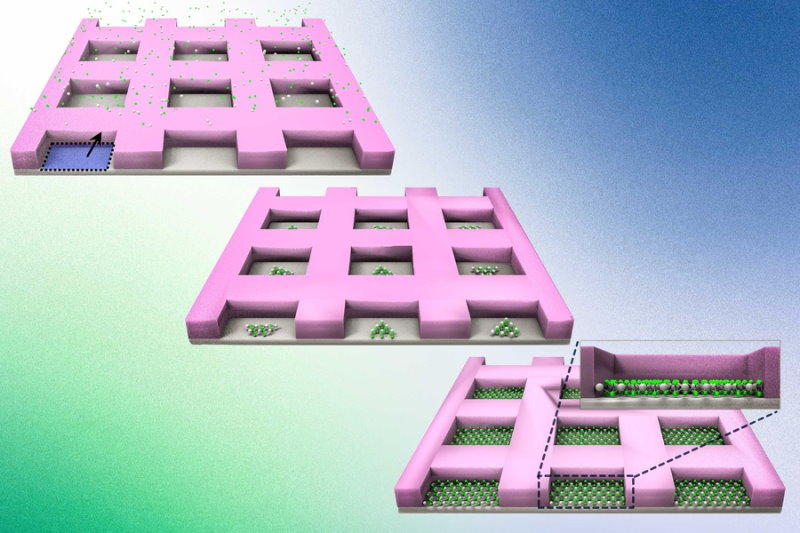
The team from MIT found a way to align the crystal growth of TMDs on silicon. Using silicon dioxide as a mask material, the researchers patterned a square grid on the wafer. As gaseous precursors flowed across the wafer, atoms settling on the silicon would nucleate crystal growth inside the tiny grid pockets. This corralled the atoms and encouraged them to assemble on the silicon wafer in the same, single-crystalline orientation.

“That’s a shocking result,” says Jeewah Kim, lead author of the study published in Nature. “You have single-crystalline growth everywhere, even if there’s no epitaxial relation between the 2D material and silicon wafer.”
With their masking method, the team fabricated a simple TMD transistor and showed that its electrical performance was just as good as a pure flake of the same material. They also applied the method to engineer a multilayered device, in which a second type of TMD was grown on top of the first. This way, TMDs can be mixed and matched to obtain the desired characteristics.
“Until now, there’s been no way of making 2D materials in a single-crystalline form on silicon wafers, thus the whole community has been struggling to realize next-generation processors without transferring 2D materials,” Kim says. “Now, we’ve completely solved this problem, with a way to make devices smaller than a few nanometers.”


