Software engineers will love our automotive embedded MRAM, says NXP
Your future car will keep improving during its lifetime. Receiving updates over the air, it will perfect its safety features, get new personalization options for the dashboard layout or simply fix that annoying gap in the windshield wiper interval. As exciting as that sounds, however, you probably aren’t looking forward to having to delay your departure because your software-defined vehicle needs to update – again!
And you won’t have to, say NXP and TSMC. The Eindhoven-headquartered chipmaker and its manufacturing partner have announced the introduction of automotive processors equipped with embedded magnetoresistive random-access memory rather than flash. Thanks to MRAM’s much higher write speeds, updates will take mere seconds. And the emerging memory has plenty more to offer – also for software engineers and architects.
Perfect replacement
In a way, MRAM is a much-refined version of magnetic-core memory, the clunky ferrite-based modules that served as the world’s predominant RAM before the advent of SRAM and DRAM. At its core, MRAM consists of two magnetic thin layers separated by an insulating layer. Reading amounts to measuring the resistance of current passing through this stack – it will be high if the layers have opposite spins and low if the spins are the same. Writing involves flipping the spin in one of the layers.
Commercial development of MRAM started in the 1990s. One of the front-runners was Motorola, whose semiconductor spinoff Freescale was acquired by NXP in 2015. Long before that merger, however, the MRAM activities had already been divested as Everspin – a company that’s still around. The advantages of mainstream flash and DRAM, not to mention the cost benefits that come along with the sheer scale of their mass adoption, have kept MRAM in a niche role.
Nonetheless, Freescale’s (later NXP’s) automotive engineers have always kept an eye on MRAM, says Jeff Cunningham, NXP’s Advanced Technology Automotive director. By the middle of the last decade, that interest spiked as a technology transition was becoming visible on the horizon in the automotive IC domain: the move from bulk to higher-performance FinFET technology.
“In automotive, we’ve been used to running bulk processes of 28nm and above. E-flash works pretty well for these technologies, but it doesn’t scale well beyond 28nm, because it requires voltages of 9 volts or even higher for erase operations. That’s not compatible with FinFET. It’s possible, but it’s so expensive in terms of silicon real estate that it doesn’t make much sense to keep it monolithic,” Cunningham explains.
In other words, to reap the benefits of migrating to higher-performance FinFET technology for automotive processors, a replacement for flash had to be found. As MRAM’s characteristics started to crystallize, NXP’s engineers realized that MRAM was a perfect fit with the software-defined vehicle. Most car manufacturers anticipate adopting the so-called zonal architecture, in which a large central computer is connected to a series of zone controllers that handle multiple ‘local’ functions in the vehicle. NXP is convinced that MRAM is the perfect memory replacement for these zone controllers.
Balancing act
“MRAM features a write speed of 6.25 megabytes per second, about ten times as fast as flash. Additionally, it doesn’t require to be erased before a write,” says Ed Sarrat, global director of Product Management – General Purpose Automotive MCUs at NXP. In the real world, that means a 20-megabyte update will take about three seconds, compared to a minute for flash. That’s a pretty big difference, especially if the update were to fail and had to run again, all the while leaving the vehicle inoperative. In terms of access speed, MRAM and flash don’t differ significantly.
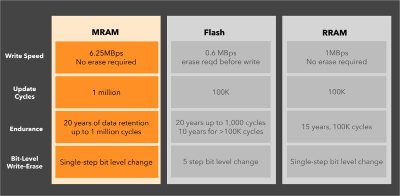
MRAM also has the edge over other memory technologies in terms of endurance. NXP communicates 20 years of data retention at a million rewrite cycles – and that’s “really conservative,” assures Cunningham. In flash, a thousand rewrites are allowed in that time span. For 10-year endurance, it’s 100k cycles.
On top of that, MRAM is expected to save on overall cost by eliminating the need for off-chip EEPROM and external data logging flash, reducing so-called keep-alive circuitry for unexpected power loss and facilitating the car manufacturing process by speeding up the programming of the electronic control units.
Finally, “software engineers are going to love MRAM,” says Sarrat. “The ability to bit-level write without requiring an erase cycle really simplifies things. You don’t have to copy the sector to RAM, erase it, make your change in RAM and write the sector back to flash. And by storing some of the data that doesn’t change as often, MRAM opens up space in SRAM. Because SRAM is expensive, it’s always a balancing act on how much can be put in. If MRAM takes some of the load off SRAM, software engineers’ job of squeezing everything into SRAM becomes much easier.”
“Since MRAM’s functionality has taken off, we see that software engineers and architects can really do great things with it. That’s one reason why we’re nerdily excited about our announcement,” beams Cunningham. Currently ironing out some final kinks, NXP and TSMC expect to start providing lead customers with the first product samples by early 2025.
Main image credit: NXP


