Explainer: how advanced packaging supports Moore’s Law
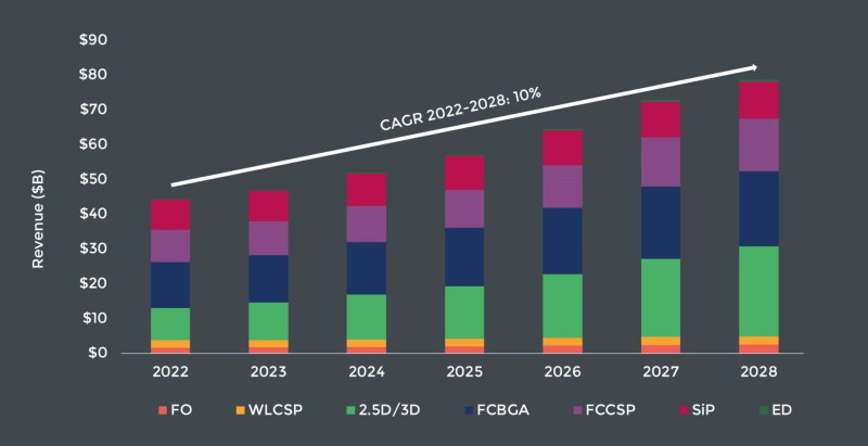
Semiconductor packaging used to be an afterthought. As a low-tech process, it was mostly outsourced to companies that compete primarily on labor costs. These days, however, leading-edge chipmakers are sinking considerable sums of money in their own packaging facilities. Their total investment amounted to 44.3 billion dollars in 2022 and is expected to grow 10.6 percent per year (CAGR) until 2028, according to Yole Group. Clearly, packaging has become a highly strategic aspect of semiconductor manufacturing.
To be more precise, a set of different techniques to combine chips into a single package – collectively referred to as advanced packaging – is booming. Next to device shrink, materials engineering and design co-optimization techniques, advanced packaging is rapidly becoming a major pillar of innovation driving Moore’s Law.

It’s not hard to see why: advanced packaging allows more transistors to work together. Over the past decades, lithographically-driven scaling has enabled the number of switches on a piece of silicon to grow from tens to billions. Now that the shrink is slowing down while chip production costs are going up, it’s becoming harder and harder to increase computing power by increasing the transistor numbers through this mechanism.
Form-factor issues aside, making the pieces of silicon bigger isn’t an attractive solution. The larger a die, the more likely it turns out to be useless because of one or more catastrophic defects. Small dies keep yields up, which is especially important considering the eye-watering manufacturing costs of modern semiconductor manufacturing. By linking up multiple dies, transistor count can continue to grow, however. Intel CEO Pat Gelsinger has promised 1 trillion transistors in a single chip package.
Another reason for introducing advanced packaging is the communication bottleneck. Just like transistors, intra-chip wiring has been scaling down to smaller geometries and tighter packing. These interconnects within chips have been getting longer as well. The resulting increased parasitic resistance and other effects introduce significant delays in the communication between different parts of a chip, up to the point that any improvement in computation speed is negated. By stacking chips and using fatter pipes to connect them, a communication bottleneck can be avoided.
Finally, as the price per transistor is no longer going down and some functions, such as I/O and SRAM, have always scaled poorly, there’s a strong incentive for chipmakers to disaggregate functions. Cutting up designs and manufacturing different functions in process technologies that are optimal in terms of cost and performance requirements keeps the appetite for scaling the logic parts strong.
Main image credit: Samsung


