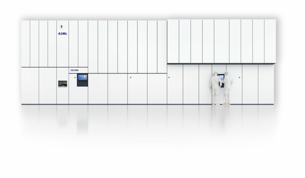
ASML: high-NA “clearly the most cost-effective solution”
The appetite of the world’s leading-edge chipmakers for ASML’s high-NA EUV systems is “healthy,” CFO Roger Dassen told Bits&Chips. The rate at which orders are coming in “matches our expectation,” he said, pouring cold water on rumors that enthusiasm for the next-generation EUV lithography tool wasn’t as high as one would expect.
Last month, the cost-effectiveness of high-NA EUV lithography for upcoming nodes was called into question. Based on lithography modeling, market research firm Semianalysis argued that dose requirements for the most complex layers were hurting high-NA throughput so much that EUV double patterning comes out on top in terms of cost, despite having twice as many wafer passes through the scanner for the same amount of chip layers.
The cost analysis seemed to be corroborated by reports that TSMC was in no hurry to adopt high-NA EUV. Last week, the Taiwanese foundry’s management did little to dispel or confirm those rumors. “We look at it carefully, look at the maturity of the tools, look at the cost of the tools. We always make the right decision at the right moment to serve our customers,” TSMC CEO CC Wei said on the Q4 earnings call, without revealing a timeline.
By contrast, Intel is hammering home the message that it intends to be the first to introduce high-NA EUV tools in high-volume manufacturing. The chip giant recently received the first shipment of high-NA components.

As soon as possible
“It’s no news to us that the higher dose needed to obtain certain critical dimensions has an effect on throughput,” Dassen commented on the Semianalysis publication. But cost per wafer isn’t merely a throughput issue, he cautioned. “Avoiding double or even quadruple patterning drastically decreases process complexity. In my view, the Semianalysis report doesn’t sufficiently take into account the value of reducing process complexity.”
Semianalysis is indeed not big on process complexity. “While reducing complexity is nice, it’s not the main driver in fab equipment decisions. Chipmakers running 1000+-step wafer fabrication processes are used to complexity. They plan fabs and purchase equipment based on cost and projected yield, on which low-NA seems to perform better.”
Dassen counters that to find out what complications high process complexity can cause, one “only needs to have a chat with Intel.” The CFO refers to Intel’s decision a decade ago to take on the 10nm node with multi-patterning rather than EUV lithography, which at the time wasn’t yet ready for prime time. The complexities of multi-patterning, along with the concurrent introduction of another couple of process technology novelties, caused Intel to stumble and forfeit technology market leadership. As ASML’s lead high-NA customer, it’s clear that the processor maker and aspiring foundry doesn’t want to make the same mistake again.
On the possible difference in the timing of high-NA adoption, Dassen said that it’s natural for customers to make different assessments on the optimal timing of high-NA insertion. “But it’s clear that a couple of customers are eager to use it as soon as possible.” Samsung hasn’t made any public announcements concerning high-NA, but it did ink a deal with ASML last month to establish a 760-million-dollar EUV process technology R&D center in South Korea, which according to Dassen has a strong focus on high-NA.
Ramp-up
In the Q4 earnings call with investors, ASML CEO Peter Wennink weighed in that “there’s no doubt in my mind that high-NA is the right choice from an economic point of view. It used to be a question some time ago, but I think everything that we’re currently seeing is that high-NA is very clearly the most cost-effective solution both in logic and memory.”
At the behest of customers, ASML doesn’t disclose high-NA orders in detail. The Veldhoven-based company mentioned a few quarters ago that the number of orders had entered double-digit territory, to which, said Wennink, “we added a couple” every quarter. ASML aims to ship ten high-NA tools this year and ramp up manufacturing capacity to twenty per year by 2026 or 2027.
Main picture credit: ASML


