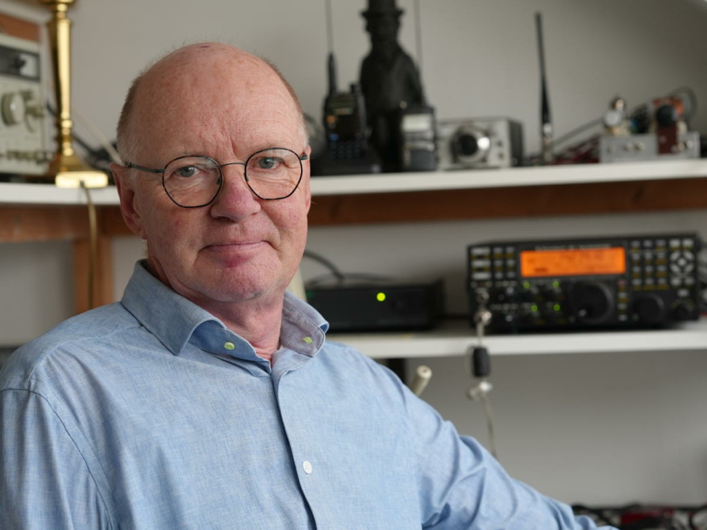
“When I talk about my own experiences, my trainees are all ears”
Jack Leijssen’s cradle literally stood on the High Tech Campus – he was born on one of the farms on the land where the Natlab emerged in the 1960s and an environment for open innovation developed after 2000. Leijssen worked at Philips all his life, as did his parents. “My mother made the PL86 television lamps as a girl, my father was employed by the Natlab. They met outside Philips and got married in 1956. A year later, I was born, so I can rightly say I come from a Philips nest,” he says laughingly.
Leijssen is a seasoned technician who was also trained within the Dutch multinational. After primary technical school (LTS), he was further educated at the company school while working at the Natlab. Following his military service, he attended the MTS and HTS, again at Philips, and took didactic training there. “Philips remained the common thread in my career: I worked in the company workshops, the production departments, the measuring room and electronics repairs.”
Very clever
After 23 years at the Natlab, Leijssen moved to the electronics department at Philips CFT in 1998. Among other things, he designed equipment for measuring interference (jitter). He was also sent by Philips to work for Bang & Olufsen for a year and a half. The Danish company truly inspired him. He was part of the team that developed the HDR1, a recorder for analog TV with an 80 GB hard disk. “You could buy it in the store. You could take it apart and I could point out the parts that contained my thoughts.”
Bang & Olufsen distinguished itself from Philips with a totally different market approach. His boss in hardware development, Pelle Nissen, once confided to him that at B&O, it didn’t all have to be so cheap; it was all about quality. When Leijssen brought up that, in his opinion, Bang & Olufsen distinguished itself through product design, Nissen told him that the difference between B&O and Philips had nothing to do with design. “That’s what everyone thinks,” he said. “Philips makes cost-optimized consumer electronics. So does Sony. We at Bang & Olufsen don’t. We want to meet our customers’ expectations.” “Well,” Leijssen replied, “so do we at Philips, but our customers’ expectations may be a bit lower, as are our price tags.”
Leijssen soon discovered that Bang & Olufsen wasn’t just selling a design experience. “They put extreme demands on EMC immunity and emission. It had to be 20 dB better than the then-strictest standard. When I reported this at CFT’s EMC Competence Centre in 2003, they just laughed in disbelief. The general opinion was that they were never going to succeed. But they did. And the remarkable thing is that they did so without industry-grade connectors. To achieve a signal-to-noise ratio of 100 dB in the audio path with just SCART is very clever.”
Warm feelings
In Leijsen’s experience, electronics was always the darling of the Philips community. CFT’s hundred-person Professional Electronics group, for example, where he worked for 23 years, was established during the infamous large-scale reorganization codenamed Centurion. “Electronics people were made redundant in all product divisions. However, they were too good to lay off, so they were transferred to CFT. What the top executives thought about that, I don’t know, but many managers must have realized that those capabilities had to be saved.”
The many reorganizations at Philips passed Leijssen by without him breaking a sweat. “I went from the Natlab to CFT on my own accord, but after that, I worked in as many as five or six different departments. It all happened to me. Suddenly, I was working at a different business unit. I opened my mailbox in the morning to discover that I had a different boss.”
A lot of colleagues were upset by the changes, but not Leijssen. “That’s the way I am. I’m into technology, and if I’m honest, everything else doesn’t interest me that much. I saw the Philips organization struggling, but I knew that the technology I was working on was sustainable. The things I liked always turned out to be useful and necessary. That’s been a constant throughout my life and my entire Philips career. My warm feelings for Philips also never suffered from all the changes and hiccups. When I retired two years ago, I knew that Philips Healthcare would continue to hire me. I’m still having a great time there.”
Regular trainer
At Philips CFT, Leijssen also developed his skills as a trainer. It all started with problems at Philips Semiconductors in San Jose. The IC designers there had developed a chip that gave EMC problems on printed circuit boards at customers. An old department manager who had been promoted to North America came up with the idea of asking Leijssen to fix the issues. “I knew him from a digital cassette project I had worked on ten years earlier.”
“The designers had delivered a good design, but they hadn’t taken into account that customers wanted to mount the chip on cheap circuit boards in a low-cost production process,” recalls Leijssen. “They had pushed all the problems out of the chip, to the periphery. As a result, the circuit board was almost impossible to make. Customers, however, want a chip in a simple reference design so they can quickly demonstrate compliance with all EMC and regulatory requirements. They don’t want a headache; they want a cheap circuit board in a cheap plastic box.”
Leijssen came up with a solution on the circuit board without requiring a new chip design and was promptly asked to train Philips employees in the US. “The initial proposal was for me to be there ten times a year for three weeks, but I was able to bring that down to five times.” He set up an EMC course and taught people at both Semiconductors (later NXP) and CFT (merged into Philips Healthcare and ASML). He became a regular trainer at Philips Centre for Technical Training and later High Tech Institute, where his course is now known as “Signal integrity of a PCB workshop.”
System-level decisions
“I particularly enjoy training because the people in my class understand what I’m talking about,” says Leijssen. “They come from a world with problems just like the ones I had. When I talk about my experiences, I notice that they’re all ears.”
The training attracts a very broad group of participants, not just IC designers but also PCB layout designers and system architects. The PCB designers especially need rules of thumb, Leijssen observes. “They have a different perspective. We have a guest lecturer in our workshop who knows their world better than I do. It involves, for example, the right selection of components and whether to put them on one or more boards.”
Leijssen especially enjoys teaching people who have to make system-level decisions. “In a low-cost design, everything has to be clearly structured together on one PCB. Unfortunately, that also means that the noise class is the same across the board. If you put a 16-bit analog-to-digital converter on there, it might only do 10 bits because it uses the same three-dimensional electromagnetic environment. In that case, it’s cheaper to use a 10-bit ADC. After all, a 16-bit result doesn’t mean you get that quality. 16 bit means a 96 dB signal-to-noise ratio. You don’t get that for free; you have to put effort into that. You have to partition for that.”
Pretty useless
Signal transmission on printed circuit boards changed significantly under the influence of CMOS chip technology. “CMOS devices became faster and faster, so the edges of the signals traversing a PCB track became steeper and steeper. The frequency spectrum required for such an edge also became wider and wider. We’re talking gigahertzes.”
In that world, a signal no longer ‘sees’ a PCB track as a capacitor that needs to be charged. “We’re now dealing with transmission lines, over which signals run like trains. Those signals have an edge that moves along the PCB track. The return current is below the edge. The signal doesn’t ‘see’ the entire capacity of the PCB track, only a small piece of about the length of the edge. Add to that that you can have multiple edges in a PCB trace. On a transmission line, that’s all on the move, traveling. It’s one of the things I cover in my workshop. You can compare it to optical signals but at about half the speed of light.”
With his training courses, Leijssen wants to get people to think differently. “Best engineering practices are pretty useless in my world,” he states. “Many electromagnetic phenomena are contrary to what your intuition tells you. People think they’re charging capacitors, but in fact, such a traveling signal on a PCB track encounters various obstacles. A capacitance here, another capacitance there. Also, the signal experiences some self-inductance. A capacitance meter might measure a 100-picofarad capacitance on a PCB trace, but a signal doesn’t see it that way. It sees distributed capacitance and distributed self-inductance. Your cell phone, all the memories, they all work with transmission lines now.”


