No technology platform can do it all in integrated photonics. In part I of a four-part series, we take a closer look at a base material that stands out for its low light losses and broad spectral coverage: silicon nitride.
In integrated photonics, you might think silicon would be an ideal substrate. After all, the ability to piggyback on decades of experience in CMOS manufacturing is a major boon. And indeed, when telecom emerged at the end of the 1990s as the first big application of integrated photonics, silicon-on-insulator photonics (SOI photonics, nowadays commonly referred to as silicon photonics, SiPh), along with indium phosphide (InP), was commercialized to modulate and convert optical signals into electronic signals, and vice versa.
SOI isn’t the only silicon option, however. As early as the 1970s, researchers started looking into silicon nitride (SiN) as an alternative base material. SiN is no stranger to CMOS, in which the material is commonly used to fabricate insulating trenches between MOS transistors. As such, SiN photonics is as CMOS compatible as SOI photonics.
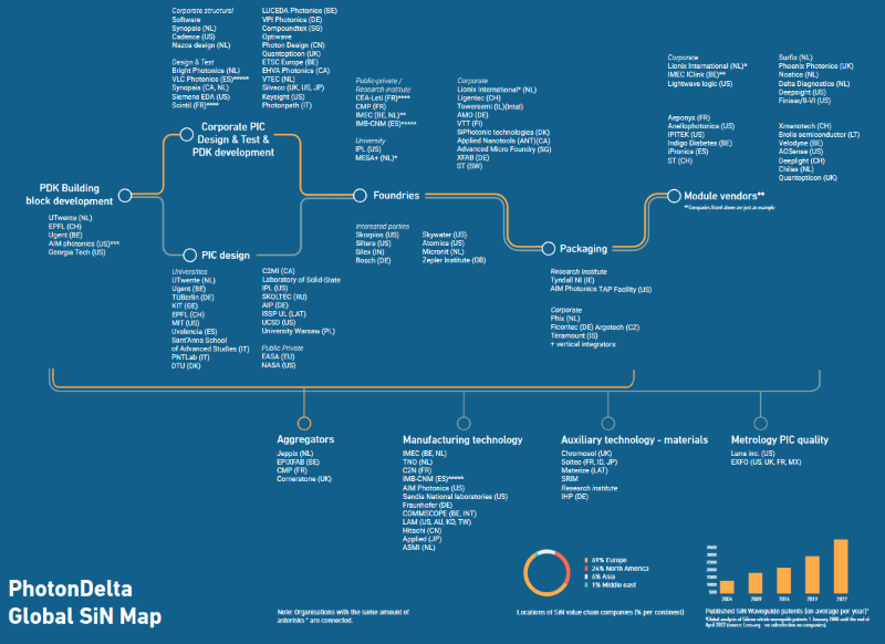
SiN is not a mere ‘SOI clone,’ however. Far from it. It has unique characteristics to offer, highly additive and complementary to the other major platforms SiPh and InP. As such, it’s not only suitable for a wide range of ‘traditional’ integral photonics applications, but it also enables a whole spectrum of new ones. By now a mature platform, thanks to the efforts of Dutch pioneer and current market leader Lionix International, SiN has emerged as a major pillar in the strategy of Photondelta, the end-to-end value chain for photonic chips, to secure a major role for the Dutch ecosystem in this budding industry. Focusing on building a library of building blocks, Photondelta is looking to become a global hub for integrated photonics.
So, what does SiN have to offer?
Blood sugar
One of SiN’s strong suits is its broad spectral coverage, spanning from nearly the UV all the way up to 2.35 micron at the edge of the near-infrared (Figure 1). Therefore, SiN is compatible with ‘traditional’ wavelength ranges used for telecom applications (1300 nm, 1520-1660 nm), but it also opens up the visible (450-750 nm) and a distinct part of the near-infrared spectrum (750-1000 nm) for business – literally.
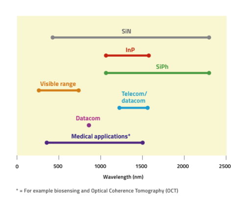
Many existing applications involving photons < 1000 nm can benefit from integrated photonics. Analytic and diagnostic systems in the life sciences, for example, rely on visible light for sensing and imaging. Introducing integrated-photonics technology helps to reduce their size, turning clunky desktop devices into handy handhelds. Integrated photonics can also improve performance, ie increase sensitivity and specificity of diagnostic tests, or improve the resolution of microscopic imaging.
In one example of miniaturization, Dutch biotech company Surfix Diagnostics is leveraging Lionix’s SiN technology to develop photonics-based disposable diagnostic tests, which can be read out in a hand-held point-of-care device and will only cost a few euros. In a doctor’s office or at home, screening for cancer could become as easy as a diabetes patient checking blood sugar levels. Surfix chose to use 850-nm near-IR light in its sensing devices because this wavelength is traditionally used for datacom applications, meaning all sorts of hardware is readily available at low cost.
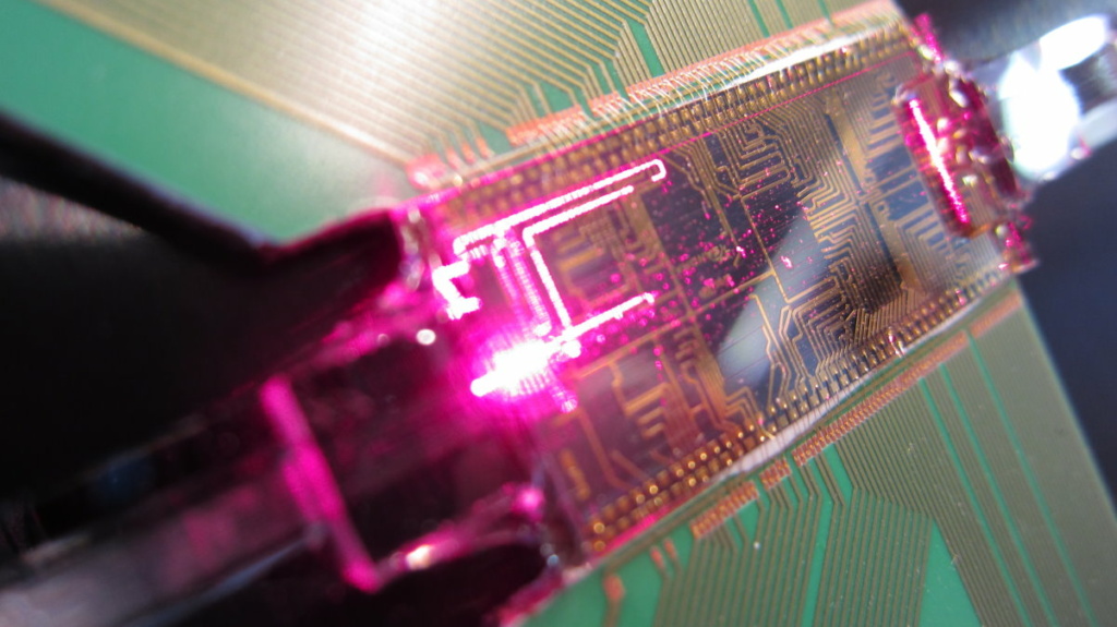
Another sub-1000-nm application enabled by SiN is augmented and virtual reality. Headset developers are eager to offer elegant and lightweight headsets but are hindered by bulky laser diodes as the only option for light sources. Lionix has integrated laser diodes, micro-optics and electrical interfaces on a millimeter-sized chip – small enough to fit on a regular pair of glasses. “We expect that these and other visible-light applications of integrated photonics will evolve to become one of the biggest integrated-photonics market segments,” says Lionix CEO Arne Leinse.
Upper limits
In addition to broad spectral coverage, SiN features low light losses. As light travels through waveguides, some of it is lost by absorption, bend losses and scattering. These losses depend on wavelength and several other parameters, but, all things being equal, they’re much lower in SiN than in SiPh and InP. Typical waveguide losses in commercially available devices are 0.5 dB/cm for SiPh and 1.5 dB/cm for InP, whereas for SiN they can go as low as 0.01 dB/cm (Figure 2). In research, 0.0001 dB/cm has already been demonstrated.
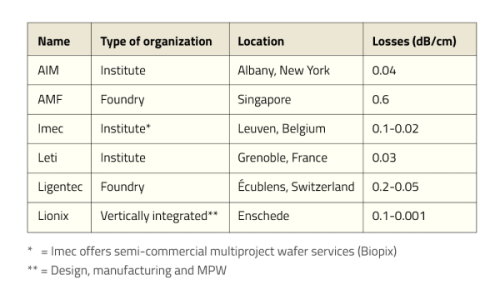
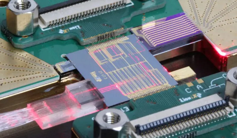
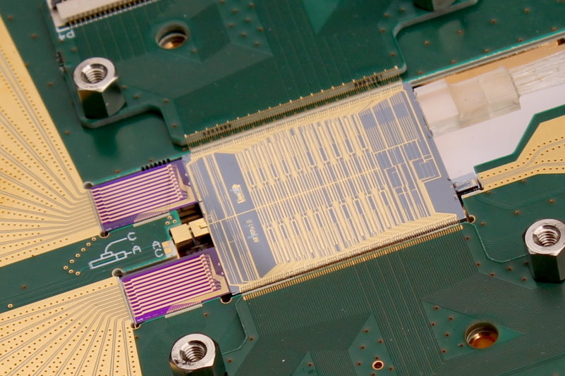
Lower light losses enable more complex circuitry. This is best illustrated by the photonic quantum computer developed by Enschede-based Quix Quantum. Photonic quantum computing involves sending photons, one by one, through an optical circuit consisting of a matrix of programmable intersections. The more intersections, the more computing power. Adding intersections, however, means increasing the size of the chip and therefore increasing the length of the path that light has to travel.
No wonder, then, that Quix’s photonic quantum processor is based on Lionix’s Triplex platform, the lowest-loss SiN technology currently available. This allows for bigger, more powerful processors.
SiN’s low light absorption, combined with its innate thermal stability, also means it can handle much higher power than other platforms. In the infrared, power levels up to 100 watts aren’t unheard of in commercial applications. In the visible range, as much as 30 watts has been reported. For comparison, for InP devices, a few hundred milliwatts is considered to be high power.
“High-power compatibility is especially important in the visible domain. The market craves compact, high-power lasers for applications ranging from laser projection displays to security scanners. The more power, the better, since every additional photon improves the signal-to-noise ratio,” says René Heideman, CTO at Lionix. “In the IR domain, too, applications such as lidar demand power levels that exceed the upper limits of integrated-photonics platforms other than SiN.”
Vast market
If, by now, you’ve started to wonder why you wouldn’t simply use SiN all the time: there are things it can’t do. As a so-called passive material, it can’t generate light on its own and, more generally, it doesn’t allow for the integration of active components. For this, it needs the assistance of InP (or another direct-bandgap material like gallium arsenide and gallium nitride). SiN therefore always needs to be combined with InP (more on that here and in part IV of this series).
SiN also has limits with respect to optical modulation. Through heating-based techniques, it’s possible to switch in the kilohertz range. Piezo-actuation-assisted switching even reaches frequencies in the hundreds of megahertz. That’s ample for a broad range of applications but not even close to the switching speeds (up to 100 gigahertz) required in telecom. Here, InP-based electro-optical modulators are used. Lithium niobate is popular too.
When SiN is an option but not the only option to realize photonic functionality, it may lose out on the other platforms because of economic reasons. For relatively modest PICs operating in the wavelength range of 1.3-1.5 μm consisting of little more than a handful of components, it makes the most sense to manufacture them all in InP, since that material is needed for the laser anyway.
At very high volumes, SiPh is unbeatable in terms of cost because these photonic chips can be manufactured in the same fabs as their electronic cousins. However, despite its historical momentum, the rationale for SiPh is shrinking, predicts Heideman. “I expect that SiN will replace SiPh in a lot of applications. After all, it’s basically the same platform, but with more advantageous characteristics.”
At least on paper, there’s a use case for all integrated-photonics platforms and all combinations thereof – the market will decide on that. However, as integrated photonic circuitry becomes increasingly complex and the application domain broadens to include visible-light applications, it’s clear that a vast market lies at SiN’s feet.
This article was written in close collaboration with Photondelta. Main image credit: Lionix

