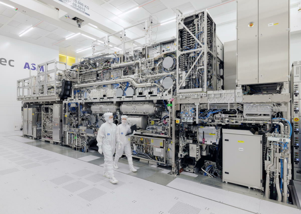
ASML will be able to contain the size of hyper-NA EUV optics by moving the last mirror closer to the wafer, R&D director Jos Benschop told Dutch newspaper NRC Handelsblad. “The downside is that more light will be reflected – as mirrors do,” Benschop said, without elaborating on how ASML intends to counteract this undesired effect.

Development and production of Hyper-NA EUV scanners is not a done deal. “When our customers need it, and when the business case makes sense, we’ll move. We have it, if you want, in our back pocket,” CEO Christophe Fouquet said at ASML’s Investor Day, held November last year. At the event, Fouquet also revealed that all EUV scanners – low-NA, high-NA and possibly hyper-NA -will in the future share a common platform. This suggests that, unlike the step from 0.33 NA to 0.55 NA, the hyper-NA mirror set is not much bigger high-NA optics.
Meanwhile, it remains unclear when high-NA EUV will be inserted in high-volume manufacturing. Intel will be offering the next-gen EUV litho technology for the 14A node, but alongside a low-NA option. At the TSMC 2025 Technology Symposium, Tuesday in Amsterdam, executive Kevin Zhang said that the firm will adopt high-NA when it “provides a meaningful, measurable benefit.” Zhang added that, at the moment, TSMC’s engineers are still able to squeeze enough density and energy-efficiency improvements using low-NA EUV.


