Your cart is currently empty!
News
SK Hynix to use Infinitesima’s AFM metrology in HBM production
Reading time: 3 minutes
The Korean chip manufacturer has ordered AFM metrology equipment from UK’s Infinitesima for the in-line inspection of high-bandwidth memory packaging, an essential part of AI systems.
SK Hynix is by far the biggest producer of high-bandwidth memory (HBM), with an estimated market share of around 70 percent. The Korean company owes this position to an early focus on mass-producing stacks of DRAM memory, achieving early successes with HBM3 and HBM3E. Now, it’s preparing to scale up volume production of HBM4E, which contains stacks of sixteen DRAM memories, using hybrid bonding as one of the packaging technologies.
Hybrid bonding is one of the drivers of the market adoption of in-line atomic force microscopy (AFM). Probably, it’s even the biggest AFM metrology market considering the amount of memory needed to power the next generation of artificial intelligence systems. Key players SK Hynix, Samsung and Micron are even looking to stack twenty DRAMs or more in future HBM generations. Six or more of those stacks are needed in an AI system.
Boost
In hybrid-bonding applications, AFM inspects the surfaces before the actual bonding step takes place. It checks the flatness of the wafer and measures how deeply the copper connections are recessed into the surface. Nanometer accuracy is required here because, in the annealing process, the expanding copper has to form a seamless joint. If the copper is too deep, no electrical connection will form. Too much copper pushes the chips apart during heating. The challenge for the AFM systems is to keep up with the rapid pace of high-volume manufacturing (HVM).
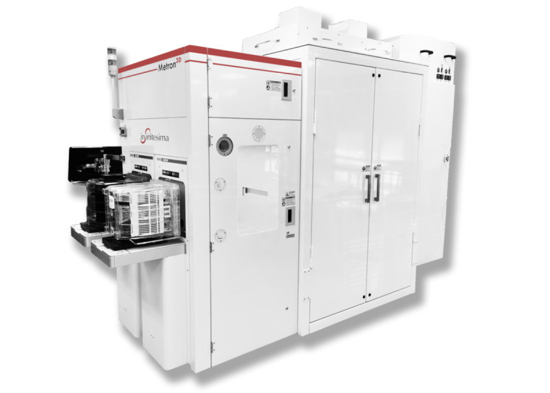
“The Metron3D system provides three-dimensional process control with sub-nanometer accuracy, crucial for fabrication of SK Hynix’s next-generation memory devices,” according to Infinitesima’s announcement. “The release to production follows an extensive evaluation period, applying the system for characterization across multiple process steps.”
The order of the Metron3D 300mm in-line wafer metrology system for volume production is a boost for Infinitesima. The announcement in itself is also significant. Chip manufacturers rarely disclose deals with their equipment suppliers because they like to keep the details of their production processes to themselves. The only reason to go public with sourcing deals is to let investors know they’re on track.
Young-Hyun Choi, responsible for defect analysis, metrology and inspection technology at SK Hynix, states in Infinitesima’s press release: “Three-dimensional process control at the nanoscale level is becoming increasingly important to ensure high yield in advanced DRAM processes. Infinitesima’s Metron3D has demonstrated excellent sub-nanometer 3D metrology with the required cost-of-ownership necessary for HVM implementation.”
Infinitesima claims the rapid probe microscope (RPM) technology of its Metron3D system provides AFM measurement capability at 10-100 times the typical AFM throughput. The system’s capabilities include fully automated wafer, data and probe handling, making it suitable for in-line volume production of semiconductor devices.
Competition
Infinitesima is in a race with Dutch Nearfield Instruments to deliver AFM metrology for in-line volume chip production. Other competitors are Bruker and Park Systems, both of which mainly serve the R&D market at the moment and seem to have been slow in entering the semiconductor market.
Last year, Nearfield also announced an order for its Quadra AFM system to be used in the production environment of a major Asian semiconductor manufacturer. In the accompanying press release, the Rotterdam-based company specifically mentioned high-bandwidth memory as an application area for the equipment. To date, only Samsung has indicated that it’s working with the Quadra machines.