From early prototypes hand-carried to customers to volume production, Xiver turns innovative microstructures into industrial-scale products for the semiconductor and photonics industries.
Imagine the windows in your office are one micrometer thick and still keep the bad weather out. Scaling down such a window structure to incredible thinness is one of Xiver’s key specialties. The membranes that the Eindhoven-based microsystems provider delivers to its customers are a prime example of that. These large-area, freestanding films, only a few tens of nanometers thick, are designed to transmit extreme ultraviolet light (EUV) but block out anything else.
The development of these EUV transparent membranes started more than a decade ago, when Xiver was still part of Philips Research. “Back then, Philips already knew how to make thin-film membranes for other applications, such as transmission electron microscopy substrates and e-beam aperture arrays. At that time, however, demands for this new application were well beyond the state-of-the-art,” says Johan Klootwijk, who was involved right from the start.
First, the membranes needed to be extremely thin to have acceptable levels of EUV transmission. Secondly, the material needed to be inert to plasma, EUV light and other types of radiation. And, lastly, the fragile membranes needed to be mechanically stable so as not to shatter during processing, assembly and operational lifetime.
“It took a few years to build the first prototype, which, after fabrication, was hand-carried to the customer’s headquarters. There, it was mounted into their machine to demonstrate the feasibility of the concept, ultimately propelling the journey of releasing these machines to volume production,” explains Wim van den Einden, process architect at Xiver. Today, Xiver’s EUV transparent membranes are in volume production and are used in fabs around the globe.
Instrumental
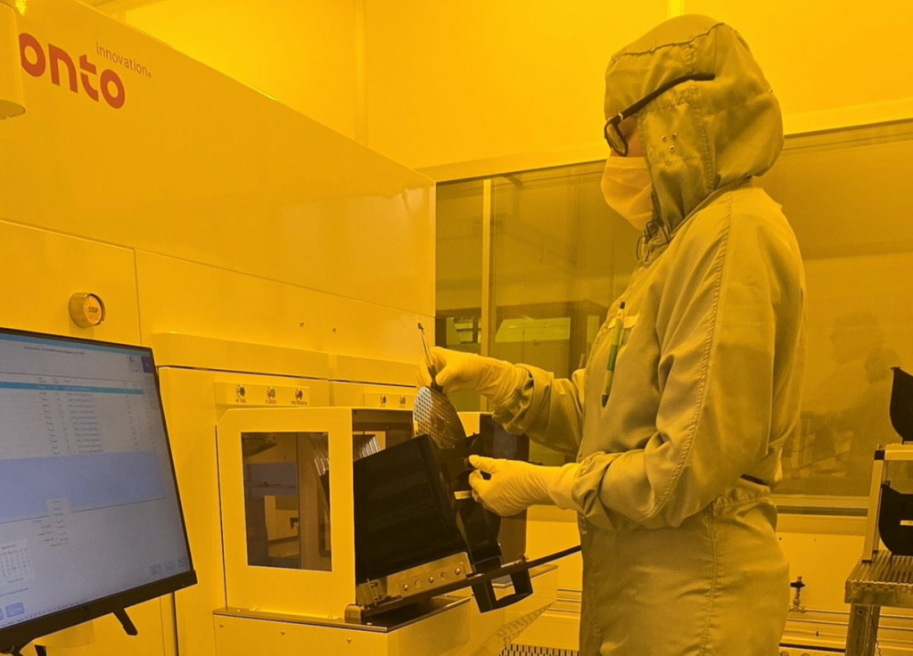
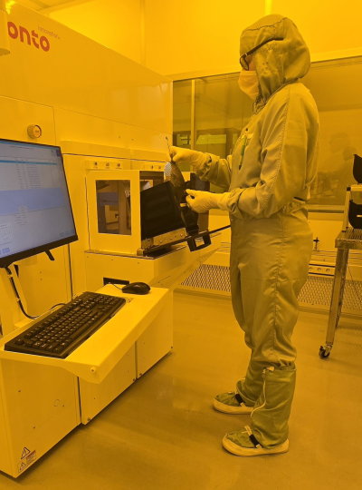
This is just one example of Xiver’s position in the semiconductor ecosystem. The Eindhoven-based microsystems manufacturer specializes in the development and production of microstructures for the manipulation of photons, electrons and ions. Another area of specialization is the manufacturing and design of MEMS ultrasound transducer arrays for on- and in-body sonography.
Some customers call upon Xiver’s innovation capabilities and drive to scale up to market-ready solutions, as was the case for the EUV membranes. Others are attracted to the unique fab manufacturing capabilities the firm offers, such as 3D through-wafer structuring and thin-film processing of ‘exotic’ materials.
For example, for another customer active in the photonics space, Xiver produces large quantities of infrared (IR) transparent silicon windows that require processing of ‘CMOS-forbidden’ materials, such as patterning of gold and platinum thin films. The High Tech Campus-based company is one of the very few wafer fabs that offer these unique manufacturing processes. “Today, we not only handle the volume manufacturing of these specialized materials but also support additional processing steps that help accelerate our customers’ production and enable them to scale their end-products to market more efficiently,” says process architect Peter van Delft.
Both the EUV and IR transmission window products illustrate how an initial customer engagement grows into a sizeable manufacturing business over a timespan of many years. “Customer engagement is often triggered by our engineering know-how. In a later stage, our fab infrastructure comes into play, along with our skillset to scale from prototype to market-ready volume production,” explains Wil van de Wiel, CEO at Xiver.
“It’s relatively easy to make an invention. It’s also relatively straightforward to run volume production of a mature product. The biggest challenge is when an innovation needs to be scaled up to production. Xiver is uniquely positioned to make this ‘lab-to-fab’ transition happen – and we have the track record to prove it,” Van de Wiel concludes. “We are and will remain instrumental in bringing breakthrough, thin-film transducer and photonic technologies to the market.”