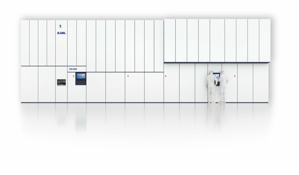
ASML’s management made short work of reports that high-NA lithography was getting a lukewarm reception.
The appetite of the world’s leading-edge chipmakers for ASML’s high-NA EUV systems is “healthy,” CFO Roger Dassen told Bits&Chips. The rate at which orders are coming in “matches our expectation,” he said, pouring cold water on rumors that enthusiasm for the next-generation EUV lithography tool wasn’t as high as one would expect.
Last month, the cost-effectiveness of high-NA EUV lithography for upcoming nodes was called into question. Based on lithography modeling, market research firm Semianalysis argued that dose requirements for the most complex layers were hurting high-NA throughput so much that EUV double patterning comes out on top in terms of cost, despite having twice as many wafer passes through the scanner for the same amount of chip layers.


