Your cart is currently empty!

Canon’s nanoimprint announcement: seeing is believing
Despite Canon’s PR suggesting otherwise, nanoimprint lithography still has a long way to go before it will be applied in semiconductor manufacturing.
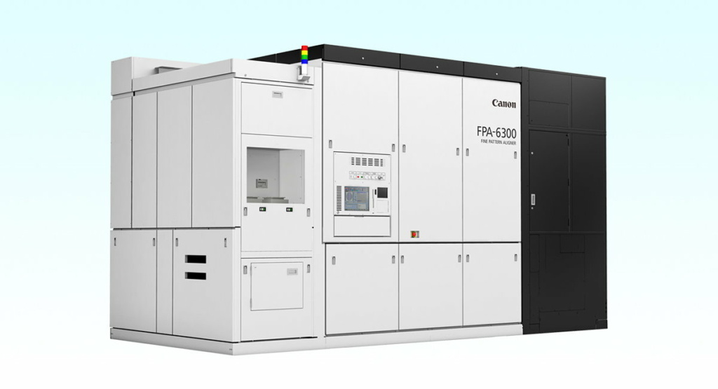
Canon has big plans for nanoimprint lithography (NIL). “By bringing to market semiconductor manufacturing equipment with NIL technology, Canon meets the needs of a wide range of users by covering from the most advanced semiconductor devices to the existing devices,” the company states in a press release, adding that its machine is capable of producing 5nm-node patterns, which will extend to the 2nm node after improvements in mask technology.
Few people believe NIL will be used to manufacture such advanced chips, or even logic chips in general, anytime soon. Even Canon itself acknowledges there are obstacles ahead. “We’re still facing challenges before we can reach the levels required for mass production,” Kazunori Iwamoto, head of Canon’s Semiconductor Production Equipment Group, told Japanese newspaper Asahi Shimbun.


