Your cart is currently empty!
Headline
Intel and TSMC go head-to-head at 2nm-ish node
Reading time: 1 minute
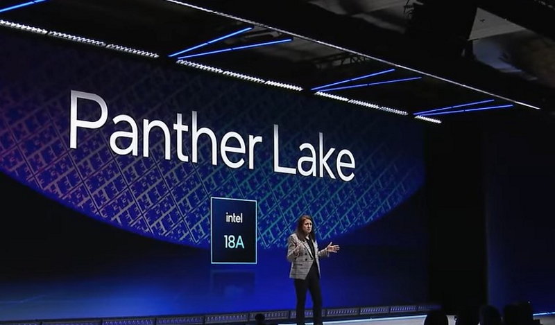
Intel has announced that its 18A node has entered risk production, meaning that the process has been frozen and the volume will be dialed up in upcoming months. Meanwhile, TSMC held a fab expansion ceremony in Taiwan, signaling the unofficial start of 2nm manufacturing.
Although the marketing-driven nomenclature suggests otherwise, Intel’s 18A and TSMC’s 2nm aren’t necessarily comparable in density, performance and power consumption. The answer to this pressing question will have to wait until the chips hit the shelves and can be compared. For Intel, the first product could be a notebook with an 18A Panther Lake processor on board. For TSMC, that could be an Apple product.
Both Intel’s 18A and TSMC’s 2nm process mark the transition from FinFET to gate-all-around technology. A notable difference is the adoption of backside power delivery by Intel.
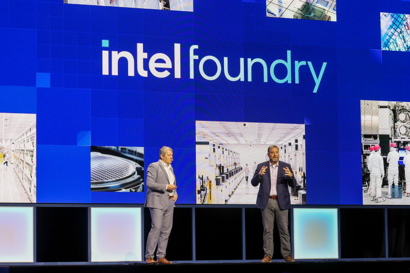
The start of the 18A ramp also marks the completion of Intel’s five-nodes-in-four-years strategy, which former CEO Pat Gelsinger put in motion to catch up with TSMC. It’s generally understood that for the firm’s manufacturing activities to stand a fighting chance, 18A needs to be a reasonably competitive product. As things stand, no major customers have placed orders at Intel Foundry.