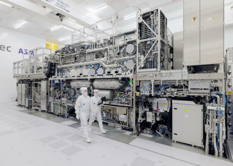
Intel has exposed 30,000 wafers on two installed high-NA EUV scanners, senior principal engineer Steve Carson announced at the SPIE Advanced Lithography Conference, held this week in San Jose. According to conference attendees’ posts on X, Carson said that ASML’s new system is performing better than expected with respect to source power and reliability.
Separately, Imec demonstrated electrical tests on 20nm-pitch metalized line structures patterned using single-exposure high-NA EUV lithography. The test tests show “good electrical yield” of over 90 percent, indicative of a low number of stochastic defects.
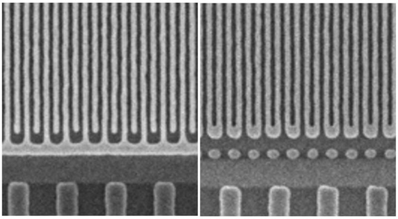
“These results represent an initial validation of the capabilities of high-NA EUV lithography and its surrounding ecosystem, including advanced resists and underlayers, photomasks, metrology techniques, anamorphic imaging strategies, optical proximity correction, as well as integrated patterning and etch techniques,” comments Steven Scheer, senior vice president R&D at Imec.
Intel looks set to be the first semiconductor manufacturer to introduce high-NA EUV into volume production. The firm last year announced that will happen at the 14A node, which is scheduled to get going in 2026 at the earliest.