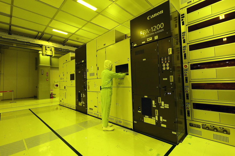
A new analysis refutes Canon’s claims that nanoimprint lithography can take on EUV.
Nanoimprint lithography (NIL) won’t be able to compete with EUV lithography in the foreseeable future. A handful of issues “without any clear way forward” stand in the way of a debut in leading-edge chip manufacturing, according to a report by Semianalysis.
NIL involves pressing a mask imprinted with the circuit pattern on a resist-coated wafer area, like a stamp. The technique was once considered a potential successor to DUV immersion lithography, but the semiconductor industry threw its weight behind EUV instead.
Canon never gave up on the technology. Initially through in-house research, later bolstered by the acquisition of the US startup Molecular Imprints in 2014, the Japanese have been developing a potential alternative to EUV for over twenty years. They launched their first NIL tool in 2023, claiming the machine is capable of producing 5nm and more advanced chips at a considerably lower cost than EUV. Canon has said it wants to sell 10-20 units annually in two to four years.
Clustered
On paper, NIL has indeed potential for leading-edge chip patterning. It’s one of few technologies that can reach ‘EUV resolutions’ in the first place without any obvious other characteristics that would make it impractical for high-volume manufacturing. NIL tools are less complex, cheaper to manufacture and use less power than EUV scanners to boot. However, after taking inventory of technical hurdles, Semianalysis concludes that NIL can’t deliver at the scale or robustness required for leading-edge logic and memory manufacturing.
One of the most fundamental problems is mask (or “template”) durability. Because the NIL process involves physical contact (pressing into the resist on the wafer), the mask’s fine 3D features are subject to mechanical stress, breakage and particle generation. According to Semianalysis, current mask lifetimes are in the order of fifty wafers in real-world use, despite optimistic claims of more than ten times that. This results in excessive mask and inspection costs.
A second key issue is overlay, or the ability to align a pattern to prior layers on the wafer. NIL overlay error is about four times larger than needed, according to analyses. Metrology improvements could offer a reprieve but would require an overhaul of the architecture of Canon’s NIL tool.
Even if the mechanics of mask life and overlay were solved, NIL still faces challenges in patterning fidelity: the creation of sharp, smooth features on the mask/template at the nanometer scale is difficult. Roughness in the mask or template translates into line-edge roughness or degradation in the printed features, which can lead to wire shorts, leakage or performance losses. The ecosystem of resist, imprint materials, curing and pattern transfer (etch/deposition) is less mature for NIL than for optical lithography, which benefits from decades of accumulated process know-how.
Finally, although NIL’s patterning tool cost and power consumption may look favorable, throughput remains weak compared to EUV scanners. For example, the Canon NIL tool is quoted at about 25 wafers per hour, or about 100 wafers per hour for a clustered setup. Today’s EUV scanners are at least twice as fast, and ASML targets 400-500 wafers per hour in a few years.
Unwarranted
The physics of contact imprinting, the fragility of masks/templates, overlay limitations, pattern-stack maturity and throughput constraints all combine to make NIL unsuitable and not cost-effective for production at the advanced nodes, where EUV will continue to reign supreme – possibly until the lithography roadmap hits a wall.
That’s not to say that NIL is useless. There are plenty of applications where it could succeed, particularly when overlay and defectivity requirements are lower, such as in less advanced logic/memory nodes, or specialty patterning of micro-optics, MEMS, sensors and metalenses. But the blanket claim that NIL will replace EUV for leading-edge nodes is unwarranted at present.
Top image credit: Canon


