Intel ditches the monolithic chip on its way back to the top
Initially, Moore’s law was principally powered by geometric scaling. Then, about fifteen years ago, chip manufacturers turned to new materials and device structures to keep it going. More recently, design technology co-optimization (DTCO) techniques have been added to keep squeezing more performance and density gains out of silicon. And pretty soon, all aspects of an entire IC-based system will need to be co-optimized, even taking into account what tasks that system needs to perform.
Of all the ways to improve IC performance, system technology co-optimization (STCO) will make the biggest difference, Ann Kelleher, head of technology development at Intel, told at this year’s International Electron Device Meeting (IEDM) in San Francisco. Kelleher’s views on the importance of system scaling echo those previously expressed by other semiconductor industry figureheads, including ASML’s Martin van den Brink and TSMC’s Mark Liu, but it’s interesting to take a closer look. After all, Intel is playing catch-up to Samsung and TSMC, and STCO may be a key element in getting back on top.
Multi-faceted
As a quick reminder, Intel lost technological leadership in the last decade. Once perceived as untouchable, the company launched its 10nm chips a stunning four years late after setting scaling goals too aggressively, allowing Samsung and TSMC to grab the lead. After taking the helm at Intel in 2021, CEO Pat Gelsinger vowed to regain “unquestioned CPU leadership performance” in 2024 or 2025.
This means Intel will need to pick up the pace. Currently, an enhanced version of the 10nm generation, rebranded as 7nm, is still Intel’s most advanced node on offer, but the Intel 4 node (which was called 7nm in the previous nomenclature) is ready for manufacturing. From this point onward, however, the roadmap accelerates to node updates every half (!) year. Development of Intel 3 (ready in H2 2023), Intel 20A (2nm, H1 2024) and Intel 18A (1.8nm, H2 2024) is “completely on track,” Kelleher told Bloomberg ahead of her IEDM keynote presentation.
For comparison, Intel’s main competitor TSMC has recently started mass-producing 3nm chips, while risk production of the 2nm node is scheduled for late 2024. Of course, node names have been marketing designations for some time, today even more so considering the multi-faceted approach to scaling. It’s therefore impossible to tell how Intel 18A will stack up against, say, TSMC’s N2.
Mix-and-match
The biggest architectural changes happen at Intel 20A, when simultaneously FinFETs get replaced with gate-all-around (GAA) transistors and backside power delivery is introduced. As the name suggests, in a GAA device, or RibbonFET in Intel’s terminology, the gate completely envelops the channel to more effectively pinch off current. It’s a natural extension of the FinFET, which Samsung introduced in mass production earlier this year (although this process is rumored to still have abysmal yield).
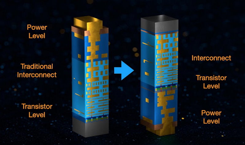
Backside power delivery (BPD), or Powervia in Intel speak, is a much more radical innovation. BPD moves power wires underneath the transistor layer, at the backside of the wafer. This reduces clutter in already overcrowded metal layers, enhances signal integrity and delivers density and power performance benefits. BPD also “gives us different opportunities in terms of what we can and how we can interconnect in the package,” Kelleher told IEEE Spectrum.

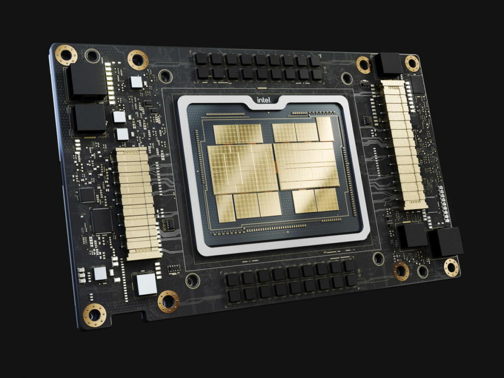
This remark alludes to what’s going to be a key element of STCO: combining multiple chips (“chiplets”) in a package. As the price per transistor is no longer going down and some functions, such as I/O and cache, scale poorly anyway, there’s a strong incentive for chipmakers to disaggregate functions into multi-chiplet bundles, in which each chiplet is manufactured using the optimal technology in terms of cost and performance requirements. Chiplets also offer a way to increase transistor count beyond what’s possible for a single die – Intel suggested in a press release that chip packages of a trillion transistors will happen this decade.
Crucially, this approach allows for blending chips from different manufacturers, allowing a combination of best-in-class dies. This is a key element in Intel’s strategy of becoming a ‘systems foundry,’ with its fabs assembling dies – only some of which may be of Intel’s making – together to create multi-chip packages.
For this mix-and-match approach to succeed, however, chiplets need to able to talk to each other as if they’re (almost) a single chip. In the race to become the technology leader, interconnect performance – latency, power use and bandwidth – will therefore become at least as important as transistor performance.
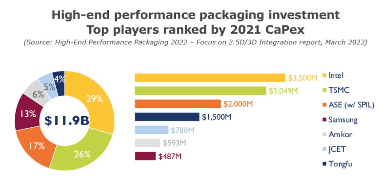
Intel already introduced several new interconnect technologies. Embedded multi-die interconnect bridge (EMIB) is a kind of silicon bridge, connecting silicon dies over short distances on the same horizontal plane in the package. According to Intel, EMIB packs interconnects more tightly than other types of so-called 2.5D packaging, resulting in faster connections. To stack dies on top of each other rather than side-by-side, resulting in even shorter die-to-die connections, Intel has developed several Foveros flavors. “Our EMIB and Foveros technologies, when combined, allow for the interconnection of different chiplets and tiles with essentially the performance of a single chip,” Intel states on its website.

Competitive edge
Chiplets are the foundation of the STCO philosophy, in which chips designers work ‘outside in.’ They start by considering workload and software, then system architecture, then selecting silicon and finally manufacturing technologies. “Essentially, one can think of STCO as assembling many technologies that once resided on entire motherboards within a single compact package. STCO starts with a perspective integrating the full functions of a system and then co-optimizes each of the components. It relies on continued progress in each individual area of the system – hardware and software – while co-optimizing holistically,” reads a paper written by Kelleher. Ultimately, “the optimization by workload and application type enables higher levels of performance and functionality to be achieved.”
STCO isn’t that different from traditional scaling, Kelleher argues; it just involves a more comprehensive perspective. “With the foundation of semiconductor processing, DTCO and now STCO becoming enhanced tools in our Moore’s law portfolio, the entire semiconductor industry will thrive by constantly leveraging each other’s unique strengths and valuable innovations. Here’s looking forward to the next 75 years of incredible human ingenuity,” Kelleher concludes.
The question is: what will be Intel’s strengths? To get back on top, it’ll still need a competitive edge in silicon or packaging technology, preferably in both. We’ll find out in the next few years.
Main image: Intel’s Ponte Vecchio processor, designed for supercomputers, combines 47 active and 16 thermal tiles inside a single package. Credit: Intel


