Is Intel’s early adoption of high-NA EUV lithography a mistake?
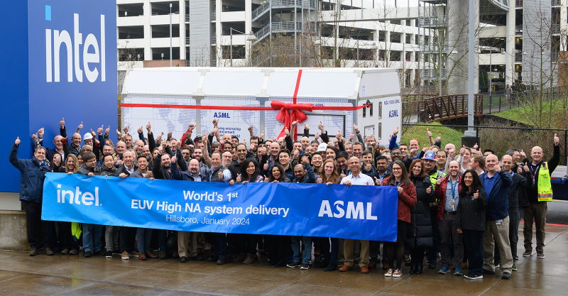
Intel has received the first shipment of high-NA EUV scanner components from ASML at its manufacturing and R&D site in Oregon, the chipmaker announced on X (formerly Twitter). The companies will soon start assembling the next-generation lithography tool, which is intended for process development. Intel will probably announce the timing of high-NA insertion into high-volume manufacturing at its Intel Foundry Services Direct Connect event on 21 February, but it will likely be around the start of 2026 at the earliest, since full-fledged high-NA production systems are expected to start shipping later this year. Reportedly, the American semicon giant will receive six out of the first ten units.
Early adoption of high NA is a key element of Intel’s ambition to regain technological leadership in the semiconductor industry. By contrast, the company was slow to adopt ‘regular’ EUV lithography, starting EUV-enabled mass production in September 2023, roughly four years behind Samsung and TSMC. Struggling with quadruple patterning and unrealistic scaling targets, Intel stumbled. After taking the helm in 2021, CEO Pat Gelsinger vowed to get back on top by delivering five new nodes in four years.
Recently, Gelsinger told investor website Barron’s that he believes Intel’s 18A node to be “a little bit ahead” of TSMC’s somewhat equivalent N2 node. Intel 18A is scheduled to enter mass production early this year and will introduce a major innovation: backside power delivery. TSMC intends on commencing production of N2 chips in the second half of 2025 but won’t start offering backside power before 2026 (Samsung hasn’t disclosed its plans yet). The Taiwanese foundry, however, says that the upcoming updates to its N3 process technology will already yield chips that are superior to Intel’s 18A products.

Lithography models
High-NA lithography, then, will be Intel’s second ace in the hole. Using high-NA tools will allow chipmakers to avoid EUV double patterning, improving design freedom, reducing process complexity and enhancing yields. These advantages come at the cost of a half-sized exposure field, which complicates the manufacturing of large dies. (By beefing up the wafer stages, ASML has prevented a huge hit in throughput.)
Curiously, however, reports have surfaced that TSMC isn’t convinced of the benefits of high-NA, at least for the next few years. “The Taiwanese firm hasn’t yet committed to high-NA EUV machines and is still evaluating the feasibility of purchasing the machines,” Digitimes writes, adding that soon-to-be CEO of ASML Christophe Fouquet is flying to Taiwan this week “to convince TSMC to adopt its new machines.”
In a separate report, published a month ago, Semianalysis questions the cost-effectiveness of high-NA tools. “Our lithography models show that despite reducing complexity, high-NA EUV single patterning costs significantly more than double patterning using existing low-NA machines for upcoming technology nodes including 1.4nm/14A. Furthermore, multi-patterning low-NA EUV is capable of finer pitch features than high-NA,” Semianalysis writes.
Slip-up
The unfavorable cost comparison is mainly the result of exponentially rising dose requirements. Printing smaller features requires higher doses of light – more photons – to prevent statistical variations from distorting the projected image. Even though ASML has been increasing source power over time, it hasn’t kept up with the increased dosage requirements, Semianalysis claims. This means that exposure time needs to go up as finer details are printed, slowing down the lithography process and increasing costs.
Meanwhile, not limited by dose requirements, 0.33-NA scanners continue to operate at maximum throughput. “The throughput advantage of low-NA double patterning is so strong that despite requiring twice as many wafer passes through the scanner, the lithography costs are lower than a high-NA single exposure. Our model shows this to be true from the current leading-edge 3nm process node out to the 1nm equivalent,” according to Semianalysis.
The report prompts some interesting questions. Is Intel, desperate to make up ground, rushing into high-NA? Or will it be able to leverage high-NA into a competitive advantage, vindicating its previous EUV slip-up? This battle will be one to watch over the next few years.
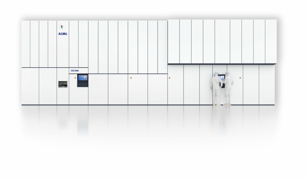
Main picture: ASML’s EXE:5000 high-NA scanner, one of which is currently being shipped to Intel. Credit: ASML


