Your cart is currently empty!
Analysis
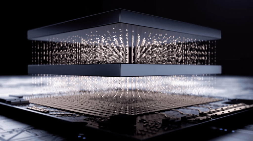
Explainer: how advanced packaging supports Moore’s Law
Reading time: 3 minutes
As the shrink slows, advanced packaging technologies allow for transistor counts to keep going up.
Semiconductor packaging used to be an afterthought. As a low-tech process, it was mostly outsourced to companies that compete primarily on labor costs. These days, however, leading-edge chipmakers are sinking considerable sums of money in their own packaging facilities. Their total investment amounted to 44.3 billion dollars in 2022 and is expected to grow 10.6 percent per year (CAGR) until 2028, according to Yole Group. Clearly, packaging has become a highly strategic aspect of semiconductor manufacturing.
To be more precise, a set of different techniques to combine chips into a single package – collectively referred to as advanced packaging – is booming. Next to device shrink, materials engineering and design co-optimization techniques, advanced packaging is rapidly becoming a major pillar of innovation driving Moore’s Law.

