Your cart is currently empty!
Imec proposes double-row CFET for the A7 technology node
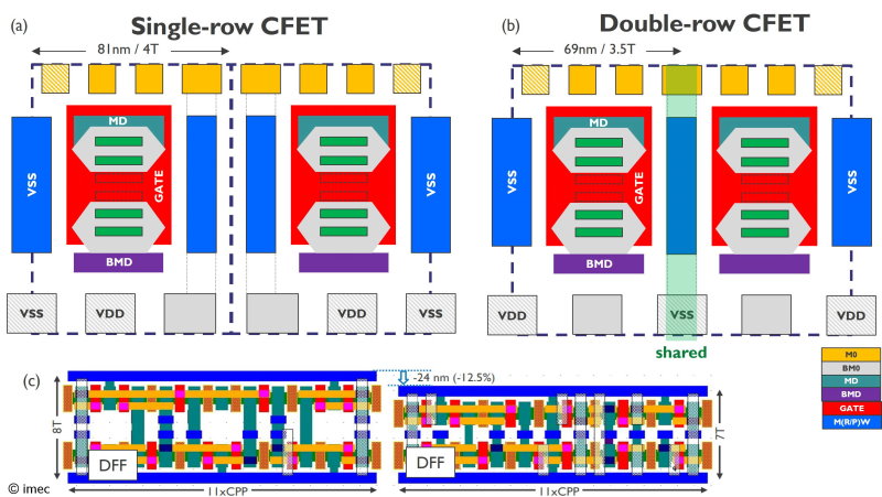
Imec has demonstrated significant logic and SRAM cell area reduction when adopting a CFET-based standard cell architecture containing two rows of CFETs with a shared signal routing wall in between. The results of the design-technology co-optimization (DTCO) study were published at the 2024 IEEE International Electron Devices Meeting, this week in San Francisco.
Stacking nFET and pFET pairs on top of each other, the complementary FET of CFET promises benefits in power, performance and area (PPA) when combined with backside technologies for power delivery and signal routing. Imec expects the CFET to be introduced in manufacturing at the A7 node, succeeding the gate-all-around (GAA).

At the circuit level, however, several options are still open for integrating CFETs into a standard cell to sustain or enhance the expected PPA benefits. Imec believes it’s come up with an architecture that offers the most optimal trade-off between manufacturability and area efficiency for A7 logic nodes.
This new architecture starts from a base cell in which one side of the CFET is optimized for power connections – including a power rail (VSS) to deliver power from the backside to the top device and a direct backside connection for the bottom device. The other side is optimized for signal connections by providing a middle routing wall (MRW) for top-to-bottom connectivity. The double-row CFET standard cell (with two rows of stacked devices) is then formed by mirroring two base cells, which share the same MRW for signal connectivity, resulting in significant area savings. Double-row A7 CFETs would enable more than 40 percent area shrinkage compared to GAA A14 node technology, says Imec.


