Your cart is currently empty!
Background
ASML Investor Day takeaways: a first step in the back-end
Reading time: 4 minutes
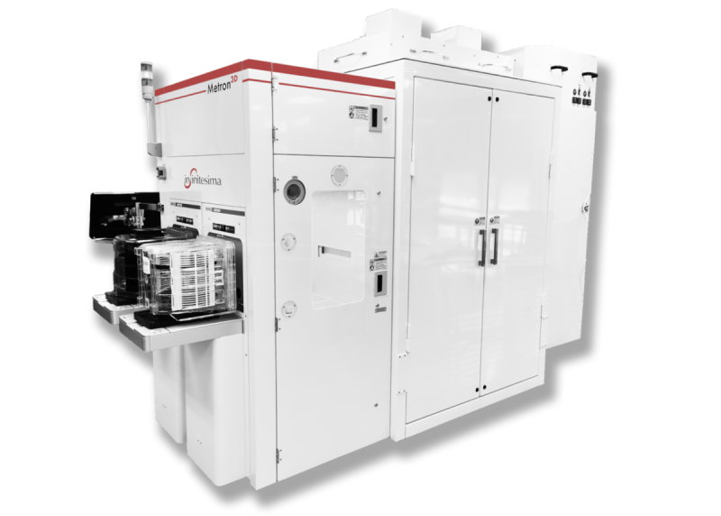
In 2025, ASML will introduce a wide-field i-line scanner, marking the firm’s first step in the back-end semiconductor market.
In 1986, ASML introduced its first wafer stepper, the PAS 2500, based on the 365-nanometer spectral line from a mercury lamp. Forty years later, the company is developing a new wafer scanner using the same i-line light, also marking a market entrance: to the semicon back-end. This world is all about combining and packaging chips. The Veldhoven-based company will ship the first tools in 2025.
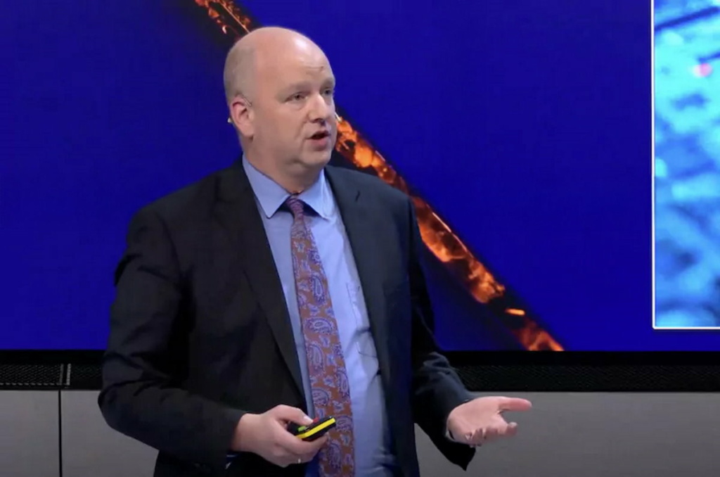
ASML’s XT:260 i-line system stands out for its high productivity. It can expose multiple fields (26 mm by 33 mm) in one scanning motion. “If you have a large field, you need fewer exposures to fill up a wafer,” EVP Business Line DUV Herman Boom explained to an audience of analysts and investors at ASML’s Investor Day, last November. “This increases productivity significantly. We’re talking about 350 wafers per hour, which is the highest productivity in the industry on an i-line system in this segment.”