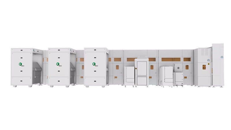
Besi and Applied Materials are expanding their partnership beyond die-to-wafer hybrid bonding. The Dutch equipment maker will join the US company’s Epic Center in Silicon Valley as an innovation partner, with engineers working alongside Applied’s teams. The expanded scope of collaboration will focus on next-generation 3D IC scaling and logic and memory integration, with expected R&D programs to include new die-on-wafer, die-on-die and die-on-panel integration platforms and photonics-enabled interconnect applications.
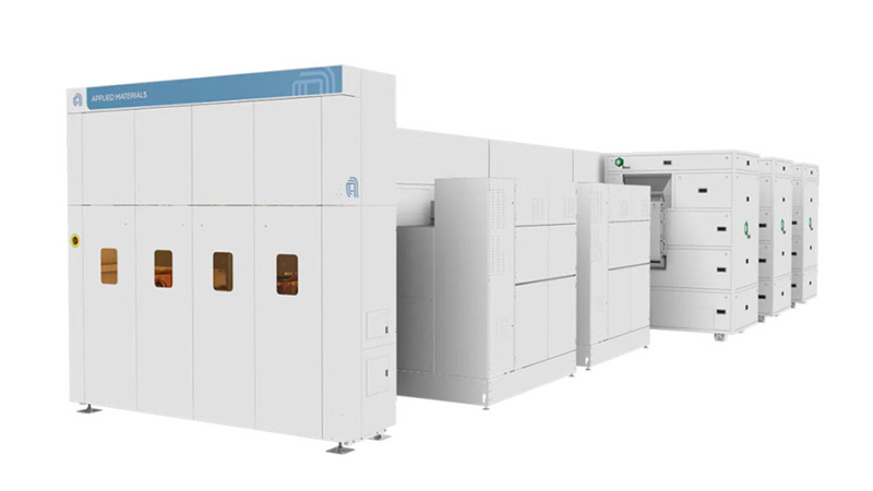
The companies began collaborating in 2020 through a joint hybrid-bonding center in Singapore. That work produced Kinex, an integrated die-to-wafer hybrid bonding system combining Applied’s wafer processing capabilities with Besi’s die placement and assembly technology.
Applied expects its Epic Center to be operationally ready this year, with capital spending rising over time to approximately 5 billion dollars. The facility brings equipment suppliers and chipmakers together to accelerate the transition from research to manufacturing.