Your cart is currently empty!
Semianalysis upholds its high-NA EUV cost-effectiveness analysis
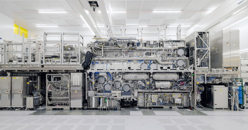
A single high-NA EUV exposure is roughly 2.5 times more expensive than a single low-NA exposure, Semianalysis concludes based on data presented by IBM at the SPIE Advanced Lithography + Patterning conference last February. As a result, high-NA EUV is the most cost-effective option only when used to replace an EUV multi-patterning sequence that involves at least three masks. The cost advantage for a four-mask self-aligned litho-etch process would be 1.7-2.1x compared to a single-pass high-NA pass.

Semianalysis made waves last year by claiming high-NA EUV wouldn’t become cost-effective until at least 2030. The market research firm argued that dose requirements for the most complex layers were hurting high-NA throughput so much that EUV double patterning remained the cheapest option. That conclusion seems to be upheld in the latest update, although as the number of exposures per layer grows, so does the benefit of switching to high-NA in terms of cost.
This analysis, as argued before by ASML and Intel, ignores the reduction of process complexity by avoiding double or multi-patterning. Semianalysis previously downplayed the benefits of process complexity reduction, and still maintains that “while reducing complexity is good, it isn’t cheaper in every case.”
All in all, Semianalysis sees only a small cost advantage for high-NA insertion for the first node at which high-NA realistically could be inserted, ie A14. As things stand, only Intel has announced concrete plans to use high-NA in high-volume manufacturing.


