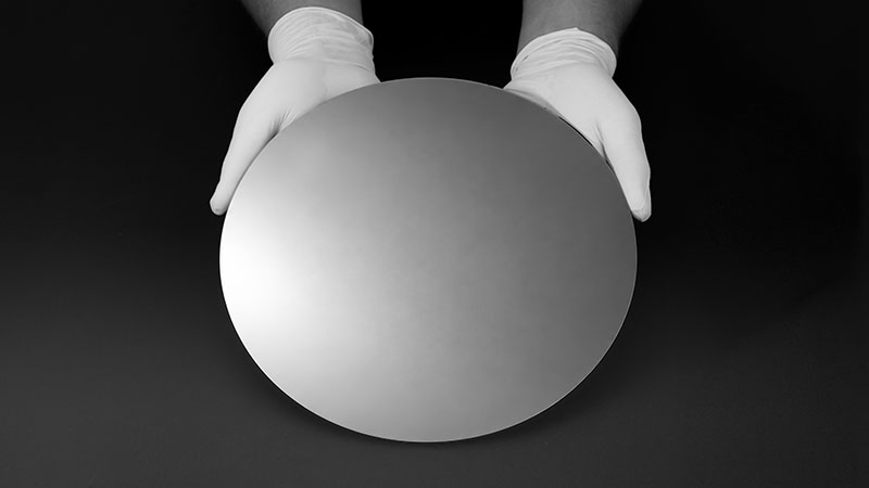
Delft-based 2D materials foundry Applied Nanolayers is seeing “a drastic increase in demand” for its wafer-sized graphene sheets, used by customers to manufacture next-generation sensing devices.
A little over a decade ago, in a bar in Leiden, the seed of a new company was sown. Over a couple of beers, two Leiden University scientists told a British semiconductor industry veteran about the work they’d been doing in the lab. Studying the growth process of graphene using scanning tunneling microscopy, the researchers had uncovered mechanistic details that allowed them to grow large chunks of high-quality graphene. Agreeing that the 2D semiconductor harbored a lot of potential as well as hitting it off on a personal level, the trio soon afterward decided to start a company and make large quantities of the material.