Your cart is currently empty!

Background
Optics drive Infinitesima’s atomic probe metrology system
Reading time: 7 minutes
Andrew Humphris’ search to capture the movements of complex biological molecules is now resulting in a tool that supports advanced semicon production. A short history and some notes about the technology behind Infinitesima’s rapid probes.
During his PhD at the University of Bristol, Andrew Humphris built scanning probe microscopes, with the goal of imaging biological structures like RNA, DNA, and proteins. At a nanometer scale, these molecules can change very rapidly. That is why Humphris started to develop fast atomic force microscope versions, systems that would be able to capture structures real time – at video speed, if you like.
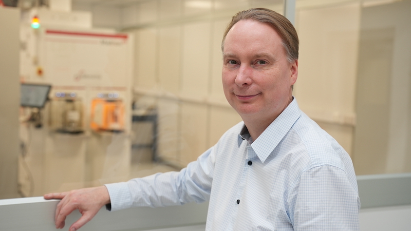
This caught the interest of fellow researchers, who became interested in the same properties. The problem: every one of them came with her or his own wish list. “Some asked me to add special electronics, others wanted special features”, says Humphris, who is now CTO at Infinitesima, the company that has its roots in his early research. The company originally focused on microscopy for R&D, and is now targeting AFM metrology for semiconductor production environments.
Humphris tells the foundation of Infinitesima was driven by a couple of reasons. “We were developing boxes of electronics within the research team, but the department became fed up with making them. The other thought was: well, if we can sell these improvements, we should start a company.”
Physics and engineering
Although Humphris had been on track for academia, securing a research fellowship after his PhD in 2001, and heading for a lectureship at Bristol, he didn’t find the choice of a career in business that difficult. “In the UK, as an academic, the teaching load can be high, and my passion was for research rather than teaching. If I hadn’t studied physics, I certainly would have chosen engineering. There’s something nice about doing something more than once and doing it reliably and repeatedly.”
Three years after its founding, the Infinitesima team grew to five people and moved into its first office in Oxford in 2004. In the following years, they demonstrated a model in which an imaging probe works closely together with an integrated interferometer. The following addition of photo-thermal actuation of the cantilever tip with a laser significantly accelerated the nanoscale measurements. During these early years, the technology also attracted attention outside the biological field. Humphris: “At a number of conferences, we received a lot of interest from semiconductor researchers.”
Vacuum compatible
Some early partners saw the potential of the technology and encouraged Infinitesima to develop RPM modules that could be integrated into equipment for the semiconductor space. That’s why the UK company started to develop vacuum compatible versions of the technology. One semiconductor manufacturer introduced Infinitesima to Carl Zeiss. There was a need for a combination of the RPM-technology in the repair for upcoming EUV masks. Working with the Zeiss teams based in Jena and Roßdorf (near Darmstadt) this led to the first RPM shipment on the Merit next Mask Repair system from Carl Zeiss, and in this way produced some initial business.
A few years later, Hitachi integrated the module in a state-of-the-art defect review SEM that was shipped in 2018 to ‘a leading logic manufacturer’ in the USA.
Integrating modules for hybrid applications in other platforms is quite an engineering challenge. It is a niche market, certainly in the mask area, and is hard to scale as a business. These projects however provided the opportunity to develop and mature the core technology.
Second hand Nanometrics platform
The focus on the semiconductor market gradually increased. A major step was building a demonstrator platform on top of a second hand Nanometrics metrology system that Infinitesima bought. “We mounted our rapid probe microscope (RPM) and started running wafers”, says Humphris. “We were really dependent on the early interest and willingness of people to send wafers, and on their interest in the data that we were creating.”
This proved to be a real confidence builder. “Seeing wafers coming in, seeing the interest—it gave us the belief to invest in building a full system.” At that time the team had grown to about 25 people.
Process control
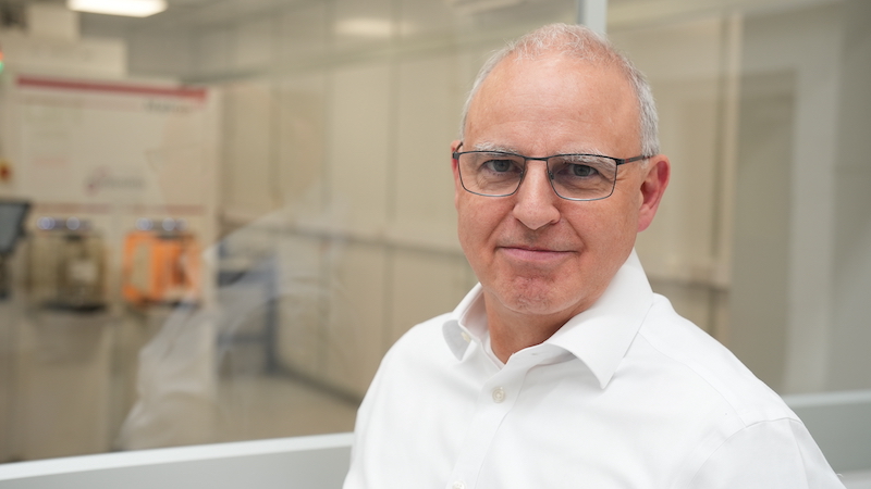
By the time the current CEO Peter Jenkins joined the company in 2019, Infinitesima saw the potential for the technology in process control for wafer fabs. “If we could take the technology directly into the semiconductor manufacturing environment, that would offer us a much bigger market,” says Jenkins who explains more about his strategy and the AFM metrology market in a separate interview.
Jenkins fortunately started at Infinitesima just before Covid hit. Together with Humphris, he took the opportunity to personally visit Intel, Samsung, TSMC and other key players, to explain what they were aiming at with their Metron system, and to get feedback from potential clients. “It was hugely beneficial to have entry points that we could talk to, before Taiwan and Korea locked down. We could also start to get wafers sent, to prove our technology when the Metron system was introduced.”
In this way, Infinitesima pivoted to developing its own system that could handle 300-millimeter wafers in 2020. It shipped its first system to a customer in March 2023. “There’s a huge amount of learning when you put a machine in a wafer fab, and also when you prepare for it. Specifically for AFM, the environment in a fab is quite aggressive in terms of noise. AFMs are very sensitive to all vibrations, so we had to do some quick iterations on improving the acoustic isolation and understanding how the active pedestals operate and contribute to the stability of the system.”
600 kilohertz
Infinitesima’s rapid probe microscope uses two optical systems on the back of the cantilever. This setup provides dual signals that not only capture vertical positioning but also detects any twisting of the cantilever caused by interactions with the sidewalls of narrow structures. This results in an effective description of sidewall profiles, giving a more accurate representation of complex features.
The cantilever is actuated photo-thermally by infrared laser pulses. Jenkins: “We’re operating today at 600 kilohertz, whereas you have at best 60 kilohertz on a piezo actuation system, because of mechanical limitations. That makes us ten times faster in how we can operate that cantilever.”
Stitch images seamlessly
This speed also is the basis for superior control over the probe trajectory. “It enables a faster, safer descent into deep, narrow structures that are sometimes just 10 to 20 nanometers wide and could be 200 nanometers deep”, says Jenkins. “We can extract the depth and sidewall information without damaging the fragile probe.”
The speed advantage for large area stitching is also enabled by a large field of view of 100 microns (that of Dutch competitor Nearfield Instruments is 40 microns), which requires fewer images when inspecting large areas. Moreover, thanks to an interferometer system that tracks not just the probe tip, but also X and Y positions with high linearity across this wide area, the RPM technology can stitch images together seamlessly, to cover entire die regions.
The cantilevers with the probes are fabricated in a MEMS-proces and are microns across and microns long. Actuating these with a laser results in a much higher mechanical bandwidth than actuating them with a piezo. “With a second signal from that laser, we can actually control where the probe goes, so we can retract the probe without it interacting with features on the surface which could damage it or require it to go much slower”, adds Jenkins. “That gives us a speed advantage on topographical structures and preserves the life of the probe. The combination of sensing and actuation, and the interferometer signal that’s sensing the surface, makes our system ten times faster than traditional AFM hardware.”
Multi-axial profiling
Although customers do not officially share information directly, Jenkins concludes from private conversations that Infinitesima’s systems are at least two to three times faster than Nearfields in applications such as hybrid wafer bonding.
Another strength of Infinitesima’s RPM system is its ability to perform high-speed profiling that supports process steps like chemical mechanical polishing CMP. By leveraging the wafer stage to move rapidly while collecting dense data lines, the system can detect long-range deviations across the wafer surface—particularly at the edges, where voids often form and can severely impact yield. Jenkins notes that customers increasingly demand multi-axial profiling around the wafer’s perimeter to catch subtle inconsistencies that standard approaches might miss.
Infinitesima’s system also excels in precise navigation and alignment, says Jenkins. Both are crucial for accurate metrology in advanced semiconductor processes. Thanks to its large 100-micron field of view and nanometer-scale offset capability, the system can use the probe itself to align on small features or alignment marks, and then quickly reposition to measure specific critical structures. This approach ensures that even sensitive hotspots within a device are measured consistently.
Nearfield adds speed by using a multi-head configuration but faces challenges in synchronizing multiple probes to find the exact same features simultaneously, says Jenkins. “By relying on a single probe, we avoid inter-probe geometric variation, reducing measurement errors and simplifying the overall process.”
TEM
In general AFM delivers a level of metrology detail that traditional SEM or e-beam tools simply cannot match. While SEM images primarily reveal surface patterns through material contrast, they lack direct height information and often require low accelerating voltages to avoid damaging delicate resists, which further reduces contrast and accuracy.
Without AFM fabs might resort to slower, more cumbersome methods like TEM, which can take 24 hours per cycle and provide only limited data points—hardly practical for modern high-volume production. All current alternatives typically bring higher costs or increased yield risks. “Semiconductor progress wouldn’t halt without AFM, but it would likely be slower, costlier, and less efficient”, says Jenkins. This underscores why cutting-edge AFM systems are increasingly seen not just as enhancements, but as essential tools for sustaining the pace of Moore’s Law.
See also the interview with Infinitesima’s Peter Jenkins on this website in which he shares his vision and explains more about Infinitesima’s strategy.