Your cart is currently empty!
Headline
AMAT’s pattern-manipulating tech saves on EUV double patterning
Reading time: 2 minutes
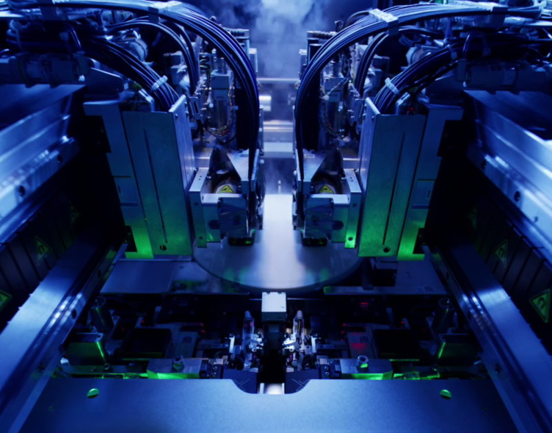
Applied Materials has unveiled a technology to replace one of two lithography cycles in an EUV double-patterning step with a single procedure. By elongating existing shapes in a specific direction, the Centura Sculpta system can bring down the space between features and increase pattern density beyond the resolution limit of a single EUV patterning step. “The new Sculpta system is a great example of how advances in materials engineering can complement EUV lithography to help chipmakers optimize chip area and cost,” said Prabu Raja, general manager of the Semiconductor Products Group at Applied Materials.
Creating chip patterns through other means than lithography is nothing new. For example, space-defined double patterning (SDDP) has been a staple in memory manufacturing for years. In SDDP, which is powered by plasma-enhanced atomic layer deposition (ALD), one lithography step and additional deposition and etching steps convert a single line into two lines, separated by a distance that’s impossible to realize with non-EUV scanners.
The Sculpta is conceptually similar: the second series of steps in an EUV double-patterning cycle is replaced by something else. Applied’s new tool directs an angled plasma beam over the wafer to remove material from the sidewalls of existing features, thus manipulating their shapes. This procedure transforms a pattern of holes into more closely spaced elliptical shapes, for example.