Your cart is currently empty!
Headline
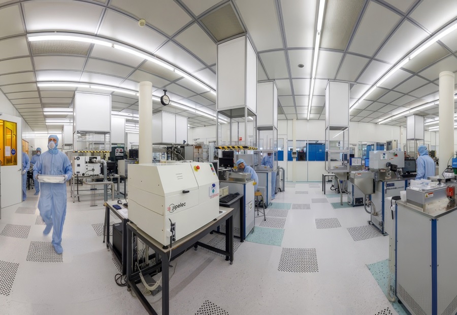
High Tech Campus welcomes Dai Nippon Printing
Reading time: 1 minute
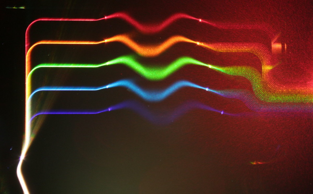
Dai Nippon Printing (DNP) will establish its first overseas research and development center in the Netherlands this September. The new facility will be located at High Tech Campus Eindhoven (HTCE), with an initial focus on co-packaged optics – a semiconductor technology integrating optical and electronic communication to deliver higher data processing performance with lower power consumption.
The first project at HTCE will be a joint research program with TNO and the Photonic Integration Technology Centre (PITC), aiming to develop package components that integrate optical and electrical circuits. Over a three-year period, DNP and its partners will pursue breakthroughs in precision patterning of optical materials. The Japanese company also considers the new Eindhoven hub as a base from which to create new businesses and forge additional partnerships.