
Even silicon starts behaving like rubber on a microscopic level. As hybrid bonding moves toward pitches of 1 micrometer and below, tiny deformations become a major obstacle. Research by Besi and Imec shows why mastering the process is just as important as building a highly accurate bonding machine.
Hybrid bonding takes place in a micro- and nanoworld in which the elastic behavior of presumably hard materials such as silicon and gallium arsenide starts becoming noticeable. The complex interaction of mechanical stress, thermal effects and bonding forces makes the introduction of this technology quite challenging.
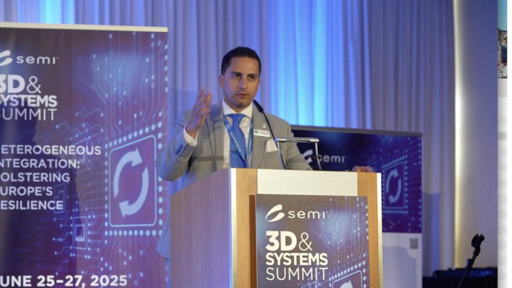
To provide some insight, Bits&Chips revisits a presentation given by Jonathan Abdilla, Director CTO Office at Besi, at the 3D & Systems Summit in Dresden in 2025. What he presented was the result of close collaboration with Imec in Leuven.