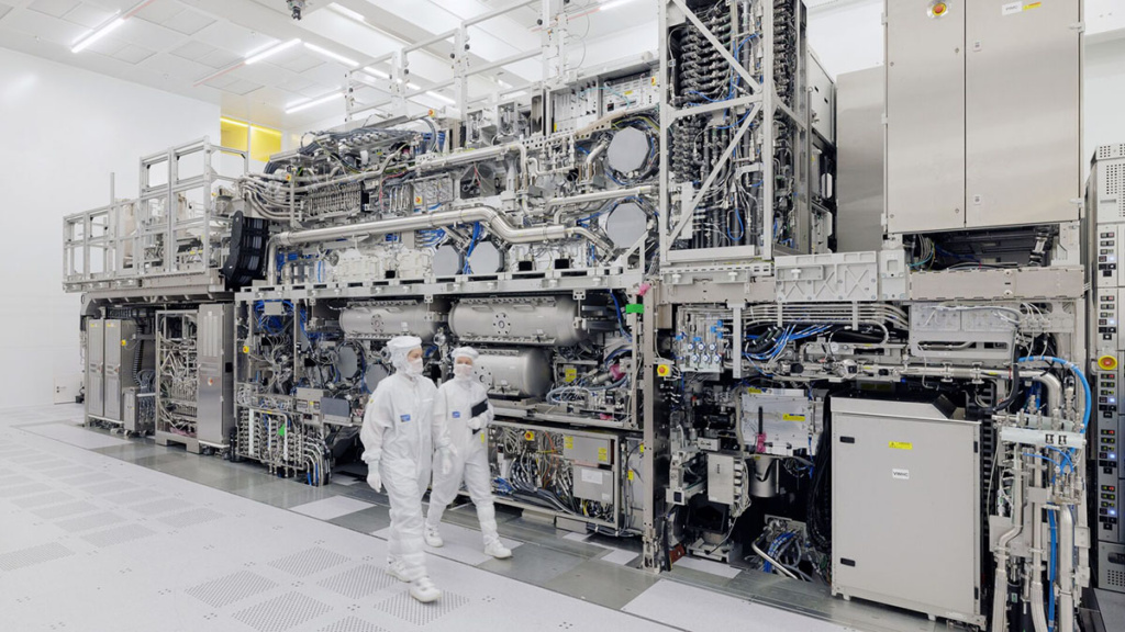
Samsung’s foundry service today announced that it is taking orders for its 5nm process, which applies EUV lithography more extensively than its 7nm predecessor. Samsung claims the new process offers up to 25 percent density improvement, 20 percent lower power consumption or 10 percent higher performance compared to the 7nm process, which entered mass production early this year. ‘Our nodes are expected to be in high demand for new and innovative applications such as 5G, artificial intelligence, high-performance computing and automotive’, says Charlie Bae, executive vice-president of foundry business. Samsung’s bigger rival, TSMC, announced commencement of 5nm risk production about ten days ago.
Headline
Samsung completes 5nm EUV development

Reading time: 1 minute