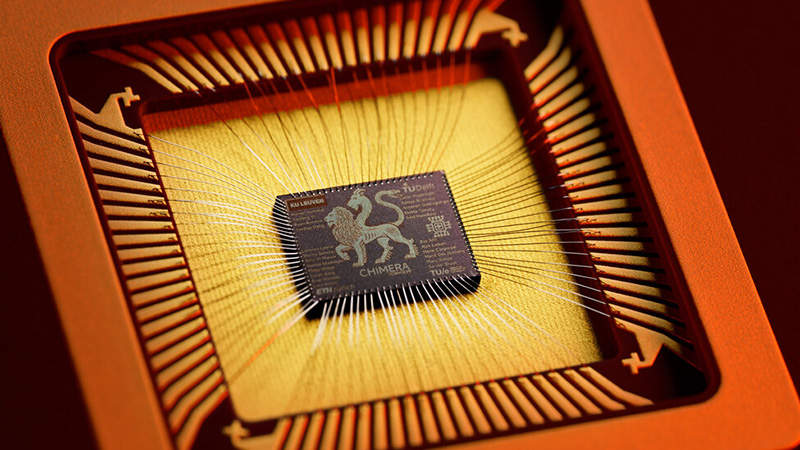
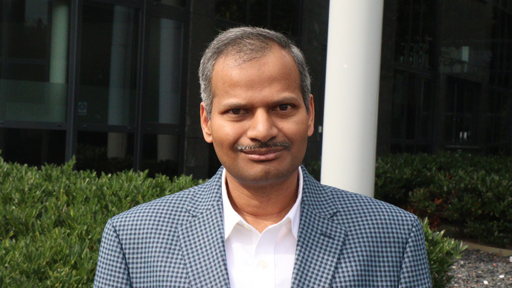
Combining components and materials makes products in high-tech systems increasingly heterogeneous. As a result, the behavior and failure mechanisms of these products are becoming more complex. Research into reliability and lifetime therefore requires combining disciplines. This should be done at Eindhoven University of Technology’s High-Tech Systems Center (HTSC), says Olaf van der Sluis. “As a mechanical engineer, I like to work with physicists, chemists and electrical engineers.”
Olaf van der Sluis worked for more than twenty years as a materials scientist at Philips (CFT, Applied Technologies, Research). There, he was involved in analyzing and optimizing a wide range of electronic products, from ICs and packages to flexible electronics and high-power LEDs. In 2010, he combined this with a part-time position in the Mechanics of Materials department at Eindhoven University of Technology’s Faculty of Mechanical Engineering. At the beginning of this year, he was given a full-time position as an associate professor. “I wanted to return to fundamental research and semiconductor applications. I also wanted to focus more on coaching students and junior researchers, such as PhD candidates.”

Multi-material, multi-scale
For Van der Sluis, the biggest challenge is that many devices combine different materials. “So, you also have different interfaces within one product. All these materials and interfaces can behave differently: brittle or tough, linear or non-linear, time and temperature-dependent, and so on. This interplay of properties means that you have to be able to predict the behavior on the different relevant scales in advance to design reliable products and complex production processes.” This not only concerns the mechanical behavior but also the physical phenomena, the chemical composition and the electronic properties.
For high-tech systems, knowledge of material behavior is becoming increasingly important, Van der Sluis states, because of the requirements for reliability, lifetime and accuracy. “Thermal problems, for example, are a hot topic, partly because high powers cause large temperature gradients. In a CT scanner or a nuclear fusion reactor, critical components are subjected to temperatures of thousands of kelvins, which causes undesirable wear mechanisms. MRI systems and electron microscopes, on the other hand, work partly under cryogenic conditions; that’s a completely different temperature range.”
“We simply don’t know enough about how material behavior changes over a large temperature range,” Van der Sluis continues. “We also have to deal with a large range on time and length scales, from nanometers to meters, and from phenomena that occur in picoseconds to lifetime estimates over years.”
Failure mechanisms
All this applies to products in use, but also during the preceding production steps, in which, for example, different temperatures can occur. “That can cause residual stresses that in turn lead to changes in material behavior on a micro-scale. Products can warp, degradation or breakage can occur or layers can come loose. And how, for example, does the heat transfer at an interface between different materials change as a result of a changing microstructure? We don’t know much about that yet.”
A few years ago, this knowledge gap became painfully clear when Philips started producing new ultrasound transducers. “They turned out not to meet the performance requirements and that was partly caused by residual stresses in ultra-thin layers that we didn’t understand. Our existing models were inadequate, we needed more knowledge. That’s why a research project was started with Philips and TUE, among others.”
Measuring these failure mechanisms may have been possible for a long time, but that doesn’t yet provide an understanding of how they arise in the production process, says Van der Sluis. “Until recently, I called these aspects secondary functionality because products are designed based on their primary function, such as computational speed or image quality. However, for the reasons mentioned, I think it’s high time to make material and interface science part of the development and design processes for high-tech systems. This is the only way to quickly arrive at an optimal design of the product and the production process.”
According to Van der Sluis, by building up material knowledge, failure mechanisms can be prevented from occurring. “If you really understand it, you can even decide to accept certain failure mechanisms. Depending on the application, you can determine when you allow them to occur in a controlled manner. On the one hand, you want to prevent failure, but on the other hand, that isn’t always necessary. You can use digital twins for this. You can use them to interactively monitor the product during use, for example to see what the temperature is doing and then keep it under control if necessary.”
Silver grains
As a concrete example of the research, Van der Sluis mentions the project that started last year with the Chip Integration Technology Center (CITC) in Nijmegen. “Together, we’re looking at a non-toxic interconnect material as an alternative to lead-containing solder. European regulations like RoHS, to restrict hazardous substances in electrical and electronic equipment, already prohibit this from being used in a number of semiconductor applications, but for power packages, for example, there’s still an exemption.”
The alternative concerns silver grains, varying in size from tens of nanometers to a few micrometers, which are embedded in an epoxy matrix. These grains are sintered into a material that, for example, connects a chip to a metal lead frame. “The sintering affects the microstructure of the interconnect material and that currently still causes adhesion problems. The adhesion between the materials is insufficient. We’re trying to establish the relationship between the microstructure, on the smallest possible scale that’s relevant, and the resulting fracture and adhesion behavior. This will ultimately enable us to design a material with the desired properties.”
The challenge lies in the complex 3D structure and the non-linear material behavior. “We’re looking for a product that meets the high requirements in terms of lifetime and reliability. For this, we’re researching additions to the silver material, such as graphene flakes or polymer microspheres. Can they change the behavior on a small scale so that we obtain the desired properties? We’re investigating this using experiments as well as theory and computer models. This combined approach leads to understanding. We’re also trying to improve the adhesion between the different layers by applying targeted structures to the surfaces.”
The collaboration isn’t limited to CITC. “We’re also talking to material suppliers because, ultimately, they have to develop and produce the new materials.”


Heterogeneous
An important development is heterogeneous integration, says Van der Sluis, outlining the broad perspective. “In recent decades, the semiconductor industry has achieved enormous miniaturization. We’ve almost reached the atomic scale and it’s becoming increasingly difficult to maintain exponential growth. One of the options is heterogeneous integration: combining different chips, with different functions, in a package or product, for example computational chips and memory chips, or photonic ICs and electronic ICs.”
The coupling of different materials leads to different interfaces, Van der Sluis explains. “That poses a challenge for the reliability, predictability, producibility and accuracy of products. All these aspects fall within our research area. Ten years ago, this was called system-in-package, now it’s even more complex. That’s why the different groups and faculties at TUE have to work together. I already realized that at Philips. As a mechanical engineer, I like to work together with physicists, chemists and electrical engineers. That collaboration is exactly what the HTSC stands for. It’s becoming more and more heterogeneous and therefore more and more fun.”
From phenomenological to fundamental
Van der Sluis is part of a broad research consortium that’s currently being formed. “Due to the demise of the Dutch National Growth Fund, we’re looking at new possibilities for financing.” He sets the bar high. “I’m convinced that this will become a major research area. For example, it’s one of the focus areas in the strategic collaboration between TUE and ASML, and it fits in with TUE’s Future Chips flagship initiative.”
His ambition is to set up a growing research group that has very strong collaborations with industry to have a major impact in that direction. “Not only to do interesting academic research but also to ensure that it lands with industry. That’s what I’ve been doing for years as a part-timer at TUE. Real collaboration, with support within the companies.”
Of course, research has been conducted worldwide for many years into the reliability and predictability of electronic products, Van der Sluis concludes. “But we add something unique by looking at the microstructure and the combination of materials and their interaction at the interfaces. This creates understanding.”
This approach is not yet common in the industry. “People research and test pure materials and products made from a single material. Don’t get me wrong, you have to keep doing that and it remains complex. But we’ve all been thinking about possible failure mechanisms for twenty years. For that, we now need to make more of a connection with knowledge of the microstructure, the combination of materials and the production processes. Indeed, then we move from phenomenological to fundamental.”
This article was written in close collaboration with Eindhoven University of Technology’s High-Tech Systems Center (HTSC).