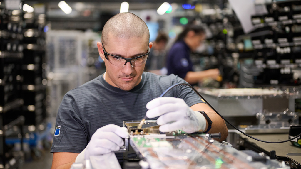

Salland Engineering, part of Japan’s Advantest since 2024, is quadrupling its test capacity. CEO Paul van Ulsen discusses the rapid changes sweeping through semiconductor testing. “We now operate as Advantest’s engineering and photonics test house.”
Paul van Ulsen still thinks it’s “incredibly cool and interesting” to lead Salland Engineering in Zwolle. When Advantest acquired his company in 2024, he agreed to stay on as CEO for another two years. For now, however, he has no intention of leaving. “As someone with a technical heart, I find it tremendously exciting to be part of all the technological craziness that’s happening.”
That excitement comes at a price, Van Ulsen quickly adds. “Everything is moving incredibly fast with AI. It’s going in every direction. The sky isn’t even the limit anymore. We really have to operate in a completely different way. In the past, we’d work through an entire project before starting implementation. For example, we used to have about three and a half months between tape-out – when a design house sends its chip to the wafer fab – and actual testing. That gave us enough time to produce and assemble the required test hardware. With that approach, we’d be far too late today. Just making a probe card for a large AI chip now takes five to six months.”
Under pressure
Lead times aren’t the only thing increasing. AI processors also require much more test time. Whereas a sizable chip might previously have spent ten or twenty seconds in a tester, the latest AI processors can already require half an hour. Add wafer and final testing together and the most complex devices can take two to three hours, according to Van Ulsen. That’s because an advanced AI processor can consist of dozens of individual dies integrated into a single package. The more complex the package, the more important it becomes to know before assembly that every individual component works properly.
“You want to be absolutely certain that those ICs and chiplets are 100 percent good before putting them into a package. So, you need to do much more wafer testing before assembly. After that, you test the complete device again.”
The required test capacity is also increasing because of the growing complexity of AI processors. They contain ever more transistors, but “you can’t simply clock such a chip faster. There’s a certain cadence at which you can run those test patterns. We’re running into limits while the chips just keep getting bigger.”
That translates directly into more machines. According to Van Ulsen, a complete tester with the necessary instrumentation can easily cost 2-3 million dollars. For some types of AI processors, manufacturers need not a handful or a few dozen but hundreds of test cells to keep up with production volumes. “That’s why Advantest is doing so well.”
The current AI boom is putting the entire supply chain under pressure. Van Ulsen sees Advantest having to supply numbers of systems that would have been unimaginable only a few years ago. “What used to be ten years’ worth of machines is now, figuratively speaking, a quarter’s worth.” He sees the same thing among industry peers. “What used to be a year’s production of probes is now being made in a month.”
The Zwolle facility has been testing AI accelerators for years, including chips from the UK’s Graphcore, Eindhoven startup Axelera and other platforms developed by European AI chip designers. Fueled by the current boom, investors are often pouring hundreds of millions of dollars or more into these tech companies.
Expanding
Advantest is the global market leader in automatic test equipment, or ATE. The market was worth about 9 billion dollars in 2025, with system-on-chip testers accounting for 6.9 billion dollars. Advantest has a particularly strong position in testers for system chips and data center memory. As AI chips such as GPUs, AI accelerators, ASICs and network processors require ever more test time, demand for the Japanese company’s testers has surged. Its share of the overall global tester market increased from 58 percent in calendar year 2024 to 65 percent in 2025. In AI chip testers, its share rose from 56 to 66 percent.
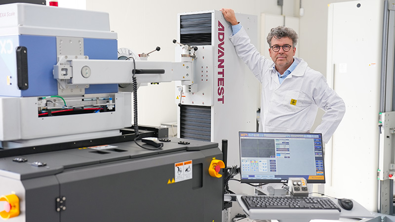
Advantest owes much of this position to its V93000 family for complex digital ICs. The company supplies these machines together with handlers, device interfaces and software as integrated test cells.
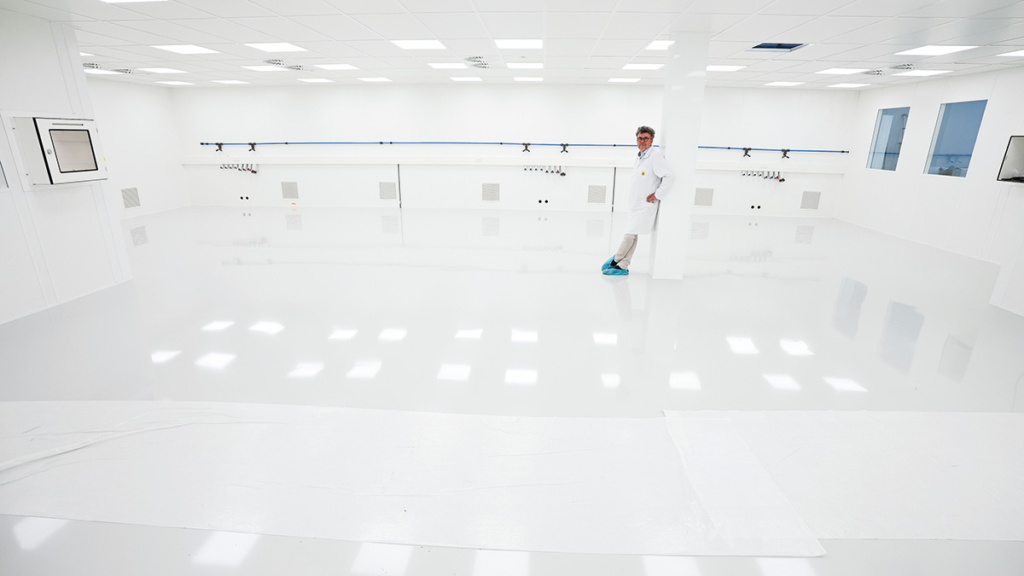
By acquiring Salland Engineering, Advantest strengthened its position in test interfaces and the associated test instrumentation. The office and test floor at the Zwolle facility is now expanding from 2,800 to 4,800 square meters. Its new 600-square-meter cleanroom will have room for ten integrated test cells.
For several years, Salland Engineering has also been developing test technology for integrated photonics and optical chips, a market in which Advantest is becoming increasingly active. That was also evident this past spring when the Japanese company entered into a partnership with Silicon Valley startup Openlight, which is working on the heterogeneous integration of III-V semiconductors and silicon photonics.
Longer waits
The increasing complexity of AI chips means work on the test hardware and probe card has to begin before the design is completely frozen. “That’s pretty crazy, of course, because designers can still make last-minute changes in the final weeks before tape-out. That’s a challenge because we have to connect their chip to the right instruments. So, for example, we need to know exactly where the connections are. While we’re developing the tests, that can still change at the last minute.”
The speed customers demand comes at a price. “We now have to come up with quick-and-dirty solutions that fit as well as possible. Only afterward do we build the final solution. Sometimes, we start things in parallel. It’s a completely different way of approaching projects. We make risk assessments in advance because things can go in several directions. It’s more expensive, but that’s what we’re seeing.”
Compared with ten years ago, the world seems to have turned upside down. Back then, every cent spent on testing was scrutinized. That world still exists, however. Cost reduction remains crucial, particularly for smaller wafer fabs. Van Ulsen describes the contrast: “At the other end of the spectrum, AI companies are spending billions. Their priority is speed to market.”
Van Ulsen observes that smaller players are increasingly losing out to the giants. “Companies with deep pockets buy up all the capacity, effectively blocking entire fabs. They also buy up all the raw materials. Smaller companies, such as a hearing-aid manufacturer, face long waiting times or can’t get capacity at all.”
Hyperscalers are also making maximum use of outsourced semiconductor assembly and test companies, or OSATs. Smaller players often find themselves at the back of the line there as well. “They impose minimum order quantities. Where OSATs used to process one lot at a time, they now want four lots at once. Otherwise, they’re not interested.”
Van Ulsen calls it a balancing act. “You don’t want to bet only on the big players because the smaller companies have often been customers for a very long time and tend to be more loyal. Sometimes, those customers grow into big players themselves. Just look at Dialog or Cambridge Silicon Radio Systems, both of which we served.”
Nanometers
Salland Engineering’s activities haven’t fundamentally changed since the acquisition. It still develops the electronics inside the tester that generate and measure signals: digital, mixed-signal, RF and optical. These days, however, Salland develops new test instrumentation almost exclusively for Advantest. Work for other companies is being phased out. “Of course, we’re only a very small part of the Advantest group, but these instruments will eventually be used in hundreds of Advantest testers. It’s enabling technology, and we develop and manufacture it in Zwolle.”
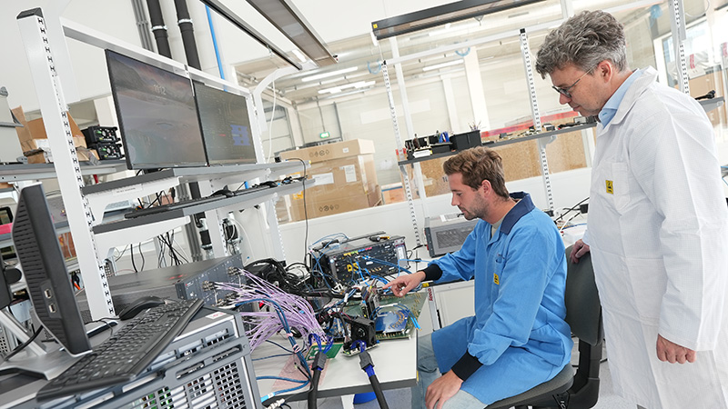
The combination of instrument development and an in-house engineering test facility was an important reason for Advantest to acquire Salland. The engineers developing the instruments in Zwolle use the technology themselves to test customers’ chips. “Because of the test house, we know damn well what actually needs to be built.”
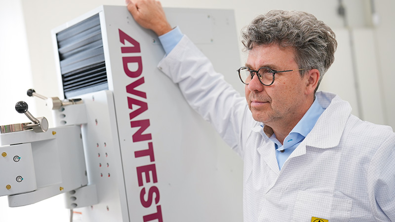
Zwolle also occupies a specific position within Advantest in photonics. Through various research and subsidy projects, Salland has built up expertise and IP for testing photonic chips over the past several years. That technology is currently being industrialized. “We now have the world’s first singulated-die handling and test system for photonics. It’s here in Zwolle.”
The chips tested by such a system have already been diced from the wafer. An individual die is picked up, positioned and then optically aligned. Coupling the light into the chip requires extremely high precision. “To test the component, you need optical alignment. You use an optical feedback loop. Only when you know you’re properly aligned can you start measuring.”
That level of precision also places demands on the environment. “You need a stable production floor. If a truck drives past, it can interfere with the measurement. We’re really talking about nanometers here.”
Van Ulsen sees Zwolle’s main role at the beginning of the industrialization curve. “In photonics in particular, we’re Advantest’s global pilot and test facility.” Requests from different parts of the organization can therefore be sent to Zwolle, where Salland develops test methods, interfaces and new instrumentation. According to Van Ulsen, the combination of application expertise and instrument development is essential.
He also sees a role for the Zwolle test facility in the Dutch photonics industry. The Netherlands and Europe have several pilot lines, but a working demonstrator isn’t yet an industrial product. “You can make a few chips in a lab. But you still have to prove that they can be manufactured in high volume.”
Testing is one of the links between research and volume production, Van Ulsen argues. A product not only needs to be tested reliably, but the testing also has to be performed within an economically acceptable amount of time. “We can industrialize test solutions for the Dutch photonics industry.”
Van Ulsen points to Phix in Enschede, which focuses on photonic chip assembly. “Phix does photonic chip assembly, we do testing. In that sense, together we’re essentially a photonics OSAT.” There’s no formal partnership yet, he stresses, but the companies are in talks and already share a customer.
Hockey stick
According to Van Ulsen, the ramp-up of assembly and testing can take place in the Netherlands. Once volumes become very large, Asia is the obvious destination. “When you get to really high volumes, we’re not going to keep that here.”
Salland uses the same model for conventional chips. Test solutions are developed in Zwolle, qualified in cooperation with Eurofins-Maser and put into small-scale production. Once the process is stable and volumes increase substantially, production can move to Asia.
“We run small series here, but high-volume production takes place in Asia. We do all the engineering needed to make a product testable. We look at how it can be tested in high volume and advise customers on what could potentially be improved.”
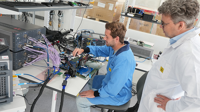
That increasingly involves substantial engineering work. For large, complex chips, the hardware between the test system and the chip is an engineering project in its own right. “The tester is standard; the interface is always custom, and we make that. We design it, make sure it gets manufactured and make sure it works. Once the entire setup works, we do the qualification and run the first production. After that, it goes to Asia.”
Van Ulsen sees little reason to install hundreds or thousands of production testers in Zwolle. Salland’s added value lies precisely in the work that comes before volume manufacturing: developing the technology, solving problems and making the test process suitable for large-scale production. “We’re at the beginning of that hockey stick.”
Rapid-response unit
According to Van Ulsen, the Advantest acquisition has significantly expanded Salland’s ability to play that role. The company now employs about 110 people, and he expects to need dozens more in the coming years. Finding those technical specialists is one of his biggest challenges.
At the same time, Advantest is investing heavily in the Zwolle operation. “I think Advantest has pumped about 15 million into the site in two and a half years, and there’s a lot more to come. The acquisition shows that there are also takeovers where the buyer doesn’t strip a company bare but instead invests heavily in it.”
The addition of 2,000 square meters of office and test-floor space should give Salland room to grow. “We have the latest Advantest equipment here in Zwolle, comparable to what the major companies have in Taiwan or the US.”
Van Ulsen likes to describe Salland as the Japanese group’s “rapid-response unit.” “If it needs to be done well and fast, they give it to us. A specification only tells part of the story. We can read between the lines and translate it into what actually needs to happen.”
Van Ulsen wants to strengthen that position in the coming years. To do so, Salland is looking for people in virtually every technical discipline: electronics, mechanics, photonics, PCB layout and signal integrity, as well as production, equipment and processes.
Van Ulsen is also keen to collaborate with universities, chip companies and the Dutch photonics industry. He mentions Smart Photonics, Brilliance and Superlight Photonics, among others. The challenges arising there could eventually lead to new instrumentation for Advantest.
This article was written in close collaboration with Salland Engineering.