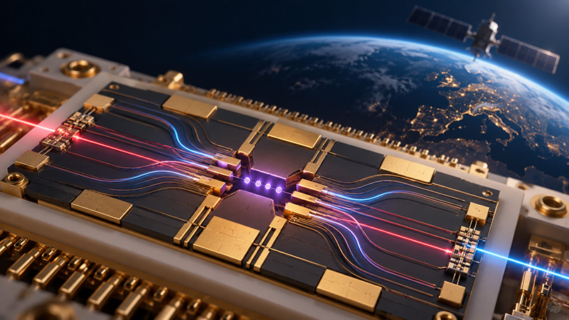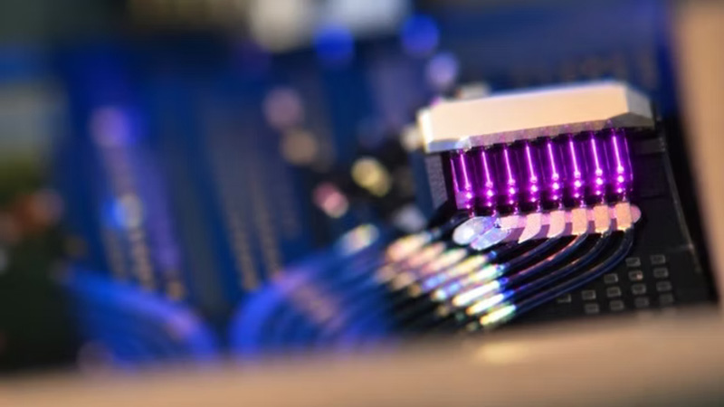
The growing maturity of integrated photonics creates opportunities for the wider Dutch high-tech industry. Not only in manufacturing capabilities like specialized equipment, manufacturing, packaging and testing, but also in system integration and the next generation of products in AI infrastructure, autonomous machines and smaller optical instruments for healthcare, agrifood and defense.
As photonic integrated circuits move into products, they need reliable supply chains and manufacturing processes that can deliver the required quality, quantity and price. The Dutch high-tech industry has many of the capabilities needed to support that transition, including expertise in semiconductors, high-tech equipment, precision engineering, systems development and research. Bringing these capabilities together can create high value for Dutch high-tech by making competitive products at scale.
Photondelta’s Future Solutions program is designed to develop the supply chain needed for the production of photonics chips, tailored to the customer needs, at scale. It starts with what a product must deliver, then connects the research, design, manufacturing and supply-chain capabilities required to achieve it. Since no company controls every stage of the integrated-photonics value chain, this coordination helps partners address the challenges of chip development, packaging and testing together. The aim is to create a clearer route from promising technology to complete solutions that can be manufactured at scale, opening opportunities for companies across the Dutch high-tech industry.
Moving AI’s data
The rapid growth of AI has created enormous demand for computing power and for efficient ways to move data between processors, memory, switches and data centers. Integrated photonics can help meet these demands by combining optical communication and switching functions in compact, energy-efficient components. Moving more communication functions from electrical to optical pathways can improve bandwidth density, latency and energy efficiency as cloud and AI infrastructure expands.
The opportunity also extends to generating the data that AI processes. Photonic chips can make sensors smaller, cheaper and more efficient, while AI can translate their measurements into useful insights. Together, these technologies can help extract more value from data about crops, patients, industrial equipment, buildings and transport infrastructure by identifying patterns, predicting problems and supporting faster decisions.
This creates a reinforcing cycle: Better sensing supplies more data, AI extracts more insight and the resulting value creates demand for further sensing. Integrated photonics supports both the collection of that information and its efficient transport to computing systems. Its role therefore grows alongside AI, from measuring the physical world to moving the data needed to understand it.
Connecting AI to the physical world
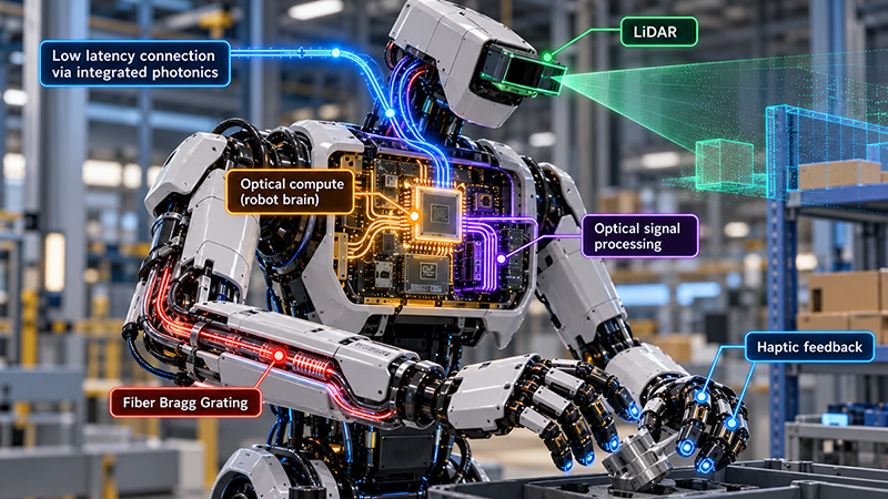
As AI moves beyond software and data centers into robots, autonomous systems and other machines, sensing and communication become part of a more demanding task: responding to the physical world. Unlike data center computing, where value is often measured in processing performance per euro, intelligent machines place a premium on low latency for safe, real-time decisions, small size and weight and energy efficiency that reduces battery and cooling demand.
The first requirement for such cognitive robotics is perception. Integrated photonics can deliver small, efficient and lightweight lidar and other optical sensing systems for depth perception, mapping, obstacle detection and localization. Other PIC-based sensing technologies can help machines detect physical, chemical and biological properties in their surroundings.
Distributed optical sensing, including fiber Bragg grating sensors, can also measure strain, pressure, temperature, vibration and acoustic signals across a machine. These measurements can support condition monitoring and predictive maintenance. Pressure and strain measurements can contribute to contact detection and haptic feedback.
The next challenge is turning this information into action. The sensors generate data streams that must reach processing systems quickly enough for closed-loop control. PIC-based optical links can move information between sensors, compute modules and actuators efficiently and with low latency. Optical preprocessing close to the sensor could also reduce the volume of data that needs to be transferred and processed.
Intelligent machines must also exchange information with other robots, infrastructure, operators and cloud-based computing systems. High-bandwidth wireless communications can support fleet coordination, shared situational awareness and access to cloud-based AI when more processing power is required. Integrated photonics can contribute across this chain, helping machines perceive their environment, connecting sensors to local intelligence and supporting communication with the wider world.
Miniaturization is a third driver for the adoption of integrated photonics into mainstream supply chains. Bringing multiple optical functions onto a chip can make systems smaller, more reliable and cheaper to manufacture and use, while reducing power consumption. Technologies once confined to laboratories or fixed installations can move into portable diagnostics, wearables, compact industrial sensors and point-of-care devices.
Healthcare offers an intuitive example. Diagnostic capabilities that once depended on centralized laboratory equipment could move closer to patients through point-of-care devices, handheld systems or even wearables. This requires optical functions previously performed by complex instruments to be integrated into smaller devices with lower power consumption, potentially improving accessibility.
Similar changes are taking place in industrial and agricultural sensing. Miniaturization changes more than a system’s physical dimensions. It changes where, how and by whom the technology can be used, potentially opening new markets.
From market demand to volume production
These opportunities demonstrate why industrialization is becoming increasingly urgent. As photonic technologies enter products manufactured in significant volumes, yield, reliability, repeatability, manufacturability and cost become critical. Product companies need predictable routes from design and prototyping into production, while customers need confidence that components will remain available throughout a product’s lifetime.
Scaling requires much more than photonic chip fabrication. It depends on connected capabilities across design and intellectual property, materials and technology platforms, foundry manufacturing, advanced packaging, assembly, testing, automation, equipment and system integration. Different applications require different combinations of platforms, materials, electronics and packaging. The objective is to create repeatable processes through which the appropriate technologies can be combined and manufactured economically.
That makes application requirements the logical starting point. A sensor for a wearable device, an optical link in a data center and a lidar system in a robot place different demands on their components and manufacturing processes. The supply chain must translate those demands into complete products, with the relevant partners working together from development through production.
Bringing Dutch capabilities together
The Photondelta Future Solutions program reflects this approach. Rather than starting with individual technologies, it begins with application needs and brings together the infrastructure, research, manufacturing and supply chain capabilities required to address them. This coordination matters because no company controls every stage of the integrated-photonics value chain.
The program targets building technological and industrial capabilities toward market adoption, scaling production and expediting progression from design to deployment. It provides a framework for demonstrating that the ecosystem can supply complete solutions as well as promising technologies.
This brings the opportunity back to the wider Dutch high-tech industry. Its equipment, precision engineering, packaging, testing and system development expertise can help photonic technologies meet the demands of mainstream markets. Chips alone don’t win markets; systems do. The opportunity lies in turning the Netherlands’ technological strengths into products it can reliably integrate, manufacture and scale.
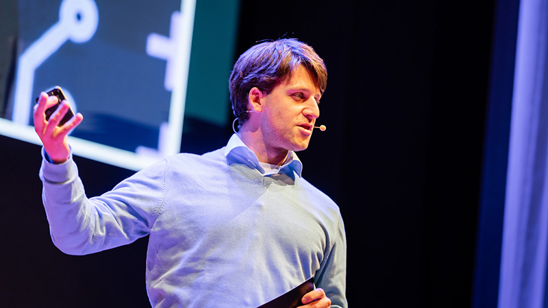
Top image: Photondelta CTO Peter van Arkel. Credit: Photondelta