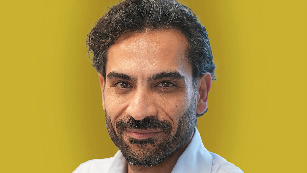
Hamed Sadeghian proposes the creation by leading Dutch high-tech players of an industrial venture for semiconductor systems scaling.
The global race for AI leadership is rapidly becoming a race for semiconductor scaling capability. Transistor scaling remains essential, but it’s no longer sufficient. The game changer in semiconductor progress will be systems scaling: how effectively chips are connected into systems. The Netherlands and Europe are uniquely positioned to lead this transition as we have all the tools and knowledge needed to win this game. We have the cards. The time to play is now.
Semiconductor scaling is increasingly becoming a system-level challenge, requiring the combined optimization of systems architecture, system integration and manufacturing intelligence. This shift, driven by AI, requires more silicon area, more wafers, more packaging capacity, more advanced interconnect capability and, critically, far more sophisticated manufacturing intelligence.
Nvidia’s system roadmap illustrates this shift clearly. Moving from Blackwell in 2025 to Rubin Ultra in 2027 increases the system from roughly 130 trillion transistors to around 1,300 trillion. This drives wafer demand from approximately 50 wafers to around 250 per system. AI scaling is therefore no longer primarily a chip design challenge. It requires advances across the entire stack, from compute and memory to packaging, data movement capacity and manufacturing precision.
The same system-level challenges are emerging across physical-AI domains, including autonomous systems, robotics, healthcare and defense applications. This means system-level scaling and manufacturing become a competitive advantage in all these markets. The Dutch and European semiconductor ecosystems are exceptionally strong in the complex equipment, process technology, photonics, precision engineering and systems know-how that make advanced semiconductor manufacturing possible. That makes them uniquely positioned to play a leading role and catch this wave.
We propose the creation of an industrial venture for semiconductor systems scaling, founded by leading Dutch semiconductor companies including ASML, ASM, Besi and Nearfield Instruments, in close partnership with TNO, Dutch universities and selected European research and industrial partners. This initiative should be supported by a scientific advisory board composed of selected fellows of the Netherlands Academy of Engineering (NAE).
Its mission should be to deliver advanced systems-of-chips as strategic products for emerging AI applications, including physical AI, by developing the systems architectures, integration technologies and manufacturing intelligence required to industrialize them at scale. Achieving and sustaining leadership in these domains will require a substantial long-term R&D capability, with Imec, TNO, universities and research partners contributing scientific excellence.
This wouldn’t be a traditional foundry fab focused on manufacturing monolithic chips. Instead, it would be a place where future systems-of-chips are architected, integrated, validated and industrialized. Similar to how leading AI companies define complete AI computing systems, this venture could position the Netherlands as a strategic systems architect and integrator for the next era of semiconductors.
In this model, Europe doesn’t need to own every transistor. It can lead in how chips become systems. For specific AI and high-performance computing applications, the venture would define the total system performance target, then decompose it into the required building blocks: XPUs, memories, integrated photonics/co-packaged optics, system fabric, advanced packaging, hybrid bonding, 3D stacking, thermal management, power delivery, high-bandwidth I/O and process control requirements.
Each component could be sourced from best-in-class global technology partners, including chips manufactured by leading foundries and IDMs such as TSMC, Samsung, Intel, SK Hynix, Globalfoundries and NXP. The strategic value wouldn’t be in owning every manufacturing step, but in owning the systems architecture, system integration know-how, interconnect strategy, system-level metrology, wafer-level process control and yield-learning intelligence to deliver the complete system-of-chips solution for AI applications.
Together with TNO, Imec, Dutch universities and the wider European deep-tech ecosystem, this creates a unique foundation for leadership in semiconductor systems scaling. The strategic opportunity isn’t to replicate Taiwan, Korea or the US and build an “us too” leading-edge fab; the opportunity is to build Europe’s leadership in systems scaling. Europe can extend its leadership from transistor scaling into systems scaling and create a new control point in the semiconductor industry. The capabilities already exist. Now it’s up to all of us to roll up our sleeves and connect them in a shared long-term industrial mission.
This is an invited editorial in response to an extensive white paper written by Hamed Sadeghian, which is available on the website of Nearfield Instruments.