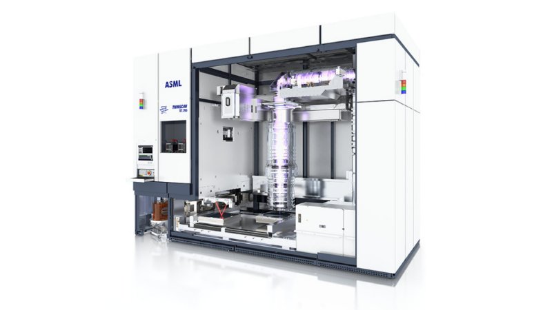
ASML appears to be developing wafer-to-wafer hybrid bonding equipment, Joo Seung-hwan of Inha University concludes following a patent filing analysis. As reported by The Elec, Joo suggests the company is adapting its Twinscan architecture for this purpose. That platform’s dual-stage design, long used to boost throughput in chip patterning, could translate into higher efficiency for wafer bonding processes.
In an interview with Bits&Chips last year, CEO Christophe Fouquet revealed that ASML is exploring opportunities in panel-level packaging, die-to-wafer bonding and, indeed, hybrid bonding. “Our core competence is accuracy at speed. That’s exactly what advanced packaging is going to require moving forward,” he said.
Hybrid bonding serves to create shorter interconnects that lower power use and increase data transfer speeds. The wafer-to-wafer variant involves connecting two processed wafers, forging dielectric and metal connections through a sequence of etching, copper filling and annealing. It’s a delicate process for which it’s not hard to see how the Twinscan dual-stage setup could be beneficial: Just as in lithography, one wafer could be subject to preparatory measurements while the other is being processed.