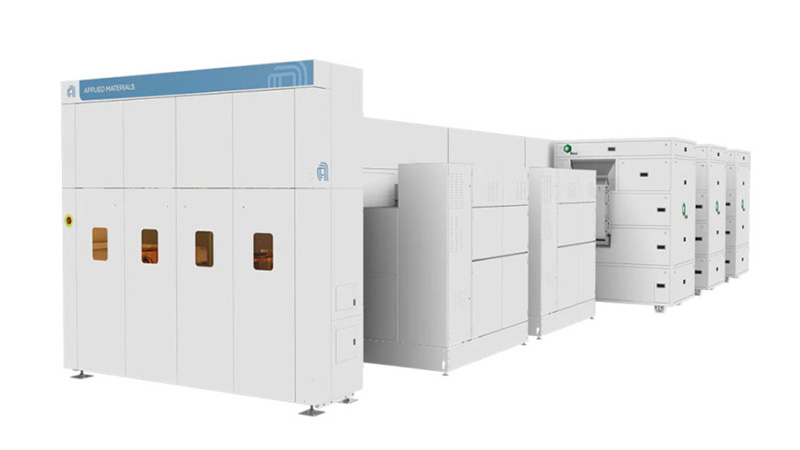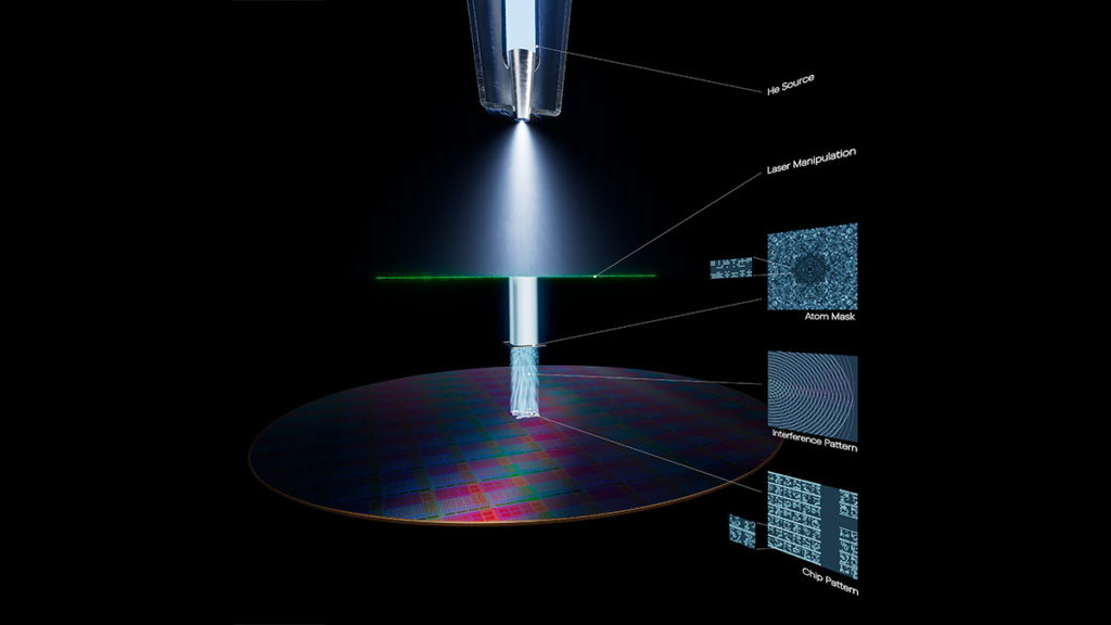
SK Hynix has effectively pushed the introduction of hybrid bonding in high-bandwidth memory (HBM) back by another generation, extending the life of microbump technology through HBM4E. The decision removes a near-term catalyst for Dutch chip equipment supplier Besi, which is betting on hybrid bonding becoming the next key packaging technology for AI memory.
Speaking at Hot Chips 2026, SK Hynix VP Jaesik Lee explained that the decision is primarily the result of a standards change. Industry body Jedec recently increased the maximum HBM stack height from 720 to 775 microns, relaxing the need for memory makers to make their dies thinner as they stack them higher. Thinner dies introduce heat dissipation issues as they comparatively contain more oxide, a poor heat conductor.
Hybrid bonding still promises significant long-term benefits, including thicker DRAM dies, lower thermal resistance and finer interconnect pitches by eliminating microbumps. But Lee stressed that producing reliable copper-to-copper bonds across 16 or 20 stacked memory dies remains a major manufacturing challenge. Currently, 12-layer HBM is in mass production and 16-layer is in customer qualification.
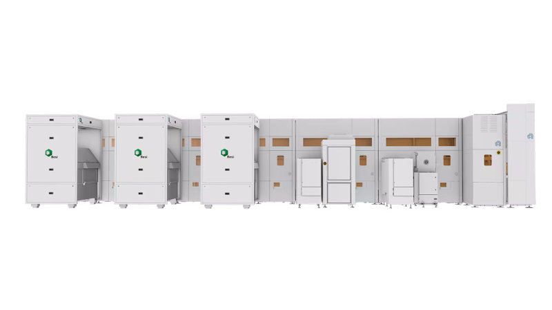
SK Hynix has reportedly ordered a pilot hybrid-bonding production line, combining equipment from Applied Materials and Besi. The Korean company’s presentation suggests follow-up orders may have been pushed out.