
Most quantum computing chips don’t work as well as they should, but nobody understands why. Leiden-based startup Quantamap is developing tools to hunt down critical defects, paving the way toward scalable chip-based quantum computing.
Semiconductor manufacturing relies on an army of metrology and inspection tools. Every critical manufacturing step is measured, monitored and optimized during production, followed by testing and inspection before chips leave the fab. Without this tight grip on the manufacturing process, today’s most advanced chips wouldn’t exist.
For manufacturing quantum computing chips, the tools developed for semiconductors don’t cut it: They either lack the relevant sensitivity or interfere with delicate quantum states. For an approach to quantum computing that’s looking to piggyback on decades of semiconductor manufacturing experience to enable fast scaling, that’s a major problem.
“The chips at the moment are just not good enough and that’s the biggest bottleneck to make quantum computing successful,” says Johannes Jobst, CEO and cofounder of Quantamap. “A lot of focus is put on how many qubits are on a chip, but the quality of the qubits is equally as important. And the qubits aren’t good enough. The more qubits you try to put on a chip, the worse it gets, both in terms of quality and yield. If the industry doesn’t figure this out, there won’t be a quantum computer that can do anything useful.”
This is where Quantamap sees its opportunity. Rather than building quantum processors itself, the startup wants to supply the tools that allow everyone else to build better ones.
Select number
Quantamap emerged from Leiden University, where its three founders crossed paths years ago. While Jobst went on to pursue a career in industry, Kaveh Lahabi and Milan Allan stayed in academia to work on quantum sensing and cryogenic scanning probe microscopy. Reunited at a party, the trio decided to commercialize a technology developed in the meantime. The university remains closely involved through research collaborations, cleanroom access and intellectual-property licensing.
The problem that Quantamap aims to tackle is that the production of quantum chips is currently best described as trial-and-error. Manufacturers complete roughly a hundred fabrication steps before packaging a chip, wire-bonding it, cooling it to millikelvin temperatures and then finally testing how well it works.
“If it’s not good enough, then what do you do?” Jobst asks. “The process chain is so complex and dependent on such subtle differences that you can’t brute-force your way out of this by trying all the parameters.” Instead, Jobst argues, manufacturers need direct insight into the physical origin of those performance limitations. “You need a microscopic picture of what’s happening on the chip to do root cause analysis and fix issues in production. If you don’t know what you made, it’s very difficult to make the right thing.”
“People have tried all the existing microscopy methods available, and they just don’t reveal the root cause. The defects that matter are the ones that survive at the deep cryogenic temperatures at which the quantum chips are operated, so you need to measure in that temperature range.”
Quantamap’s solution is as brilliant as it is obvious: Harness quantum technology to do the measurements. The firm’s core technology, which, like most quantum technologies, operates at near-zero-kelvin temperatures, is a sensor that’s essentially a close technological relative of the qubits it measures. “Whatever disturbs the qubit is also being picked up by the sensor. It’s a very natural match.”
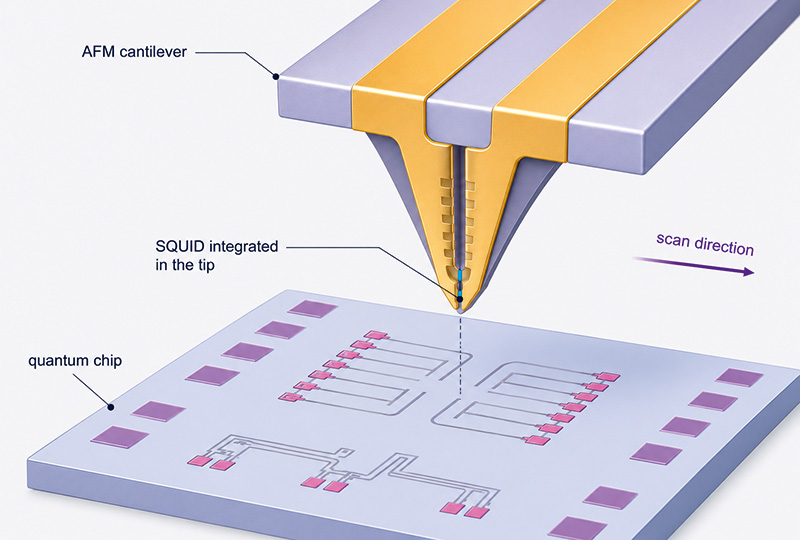
Quantamap integrates this sensor, called a superconducting quantum interference device (SQUID), directly onto an atomic force microscope (AFM) probe, allowing it to record topography and quantum-relevant properties of electric current, heat dissipation and magnetic defects simultaneously. This approach eliminates one of the persistent frustrations in scanning probe microscopy: aligning separate datasets after the measurement. “If you find a defect in your SQUID data, you don’t have to guess where it exactly is on a chip, because the acquired data includes position,” Jobst says. Capturing multiple physical properties at once also helps speed up the inherently slow nature of AFM measurements.
Currently, Quantamap is working with a select number of customers, both academic research labs and quantum companies. “These are minimum viable products. We’re aiming to launch our real product in 12 to 18 months.” The firm also sells the SQUID sensors separately and performs quantum chip measurements on demand.
Attractive
While the first order of business is to understand the nature and origin of defects, further down the road it will be necessary to prevent them from forming during the volume manufacturing of quantum chips. Due to the inherently delicate nature of quantum states, scaling production of these devices will almost certainly require even stricter manufacturing discipline than advanced semiconductors.
Providing the continuous process feedback needed to make that happen will be Quantamap’s future focus. “We want to grow up together with the quantum industry, providing in-line metrology for quantum chip manufacturing,” Jobst notes.
There is, however, an important difference between semiconductors and quantum computing. Throughput dominates semiconductor metrology because fabs manufacture enormous numbers of wafers. Quantum economics are fundamentally different. “I don’t expect we’ll ever make close to as many quantum chips as we make semiconductor chips.” Instead, Jobst envisions specialized quantum data centers rather than quantum processors inside every laptop. Quantum inspection systems, therefore, won’t need to process hundreds of wafers per hour. “If we do one wafer a day, I think we’re already doing pretty well.”
That slower pace shifts the optimization target away from throughput toward sensitivity and coverage. Each quantum chip represents substantial value, making exhaustive inspection economically attractive. “The number of chips will be lower, but every chip will be more expensive. If their yield is poor, it’s even worse than on a semiconductor line.”
Missing link
No one is making quantum chips at scale yet. But quantum computing has reached the point where incremental gains from better fabrication matter at least as much as adding more qubits. In this moment when pilot lines are being established and processors are becoming larger and more complex, understanding why individual devices succeed or fail becomes increasingly valuable. Without that feedback loop, process optimization risks becoming an exercise in educated guesswork.
As such, Quantamap could make an invaluable contribution to solving quantum computing’s scaling challenge. By providing key industrial infrastructure to quantum manufacturing, it may become one of those companies whose importance far exceeds its visibility. Every successful quantum processor would still bear someone else’s logo, but behind the scenes, the missing link between laboratory prototypes and manufacturable quantum chips might come from Leiden.
Top image credit: Quantamap. This article was written in close collaboration with Quantamap.