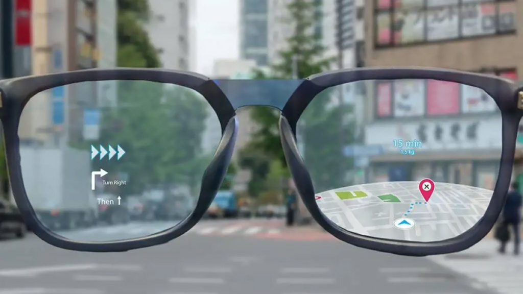
Smart glasses may need a new kind of display before they can become an everyday device. Swave Photonics is working on that challenge with holographic display technology on chip. Using Comsol simulation software, the Imec spinoff models how heat, materials and optical behavior interact before committing to expensive chip prototypes.
A decade ago, augmented reality was widely seen as one of the next frontiers in consumer electronics. Companies explored holographic displays, 3D visualization and smart glasses, but the market never took off. The hardware wasn’t ready, the use cases were unclear and smartphones were still evolving fast enough to absorb most consumer attention.
That balance is starting to shift. With smartphones now a mature platform and AI creating new ways to interact with digital information, companies are again looking at displays that can place images directly into the user’s field of view. For Swave Photonics, an Imec spinoff developing holographic display technology, that starts at the chip level.
Diego Hoffman, director of physics at Swave Photonics, came to Belgium fifteen years ago for a job at Imec. There, he was involved in different projects around electronics and microchips. Five years ago, he worked on a project to create a spatial light modulator (SLM), a chip layer that controls how light is modified across many tiny pixels. When Imec established the spinoff Swave to further develop this technology, he joined this new start-up.
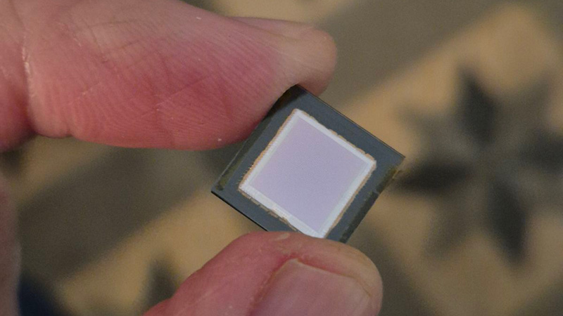
“Swave’s SLM layer has 16,000 by 16,000 pixels on a chip that’s about 5 by 5 millimeters,” Hoffman says. “The electronics layer tells the SLM how to shape the light field needed to produce a hologram.”
The small size makes the chip usable for applications like smart glasses, which is currently the main market Swave is aiming for. They see momentum here, which was lacking a decade ago.
Holographic images
Conventional techniques present the augmented reality as a 3D image by showing each eye a slightly different 2D image. Those images are presented at a particular fixed distance. They trick the brain into thinking it’s farther away. If eyes try to focus on it, they converge as if the object is at one distance, while the lens has to focus on the fixed optical distance of the display. This creates a mismatch that the brain has to solve, which can lead to nausea, headaches, tiredness and limits how long you can wear the glasses.
Swave intends to avoid this discrepancy by using holographic display technology. “To create a convincing holographic image, the chip has to control the light with enough precision for the eye to perceive depth in a natural way,” Hoffman explains. “The light behaves as if the object is there in space. So when you focus on it, the discrepancy the 2D images give won’t be there.”
The holographic images are created by local heating that changes how individual pixels modulate the light, allowing the chip to shape the light field seen by the user. These pixels operate at the nanoscale, which means the chip that produces the images needs to be very precise in where to send the heat.
Designing such a chip by trial and error would be slow and expensive. Each physical iteration requires a new chip design to be fabricated and tested, making it impractical to explore hundreds of possible geometries, materials and thermal strategies in hardware. To shorten that cycle, Swave uses simulation to predict how design choices will affect the behavior of the SLM layer before a prototype is made.
Design questions
Nano-pixel technology developers have relied on Comsol for those simulations for more than a decade. The software allows the team to narrow down the most promising designs before committing to a costly fabrication run to verify the results the software predicts. Measurements from those prototypes are then fed back into the model, gradually improving its predictive power.
“Comsol is only as good as the assumptions you put into it,” Hoffman points out. “The software solves the physics we ask it to solve. Over the years, we’ve built up models that represent our devices more and more accurately, but the engineer still has to decide what questions to ask. You choose the geometry, the material properties and the assumptions. Comsol performs the calculations and shows which adaptations are likely to give the best results. It doesn’t replace engineering.”
That interaction between engineering judgement and simulation is especially important because Swave’s chip is a multiphysics problem. Electrical control, heat distribution, optical behavior and material endurance aren’t separate questions. A change in one domain can affect the others. For example, a design that improves optical performance may require a different thermal profile and, in turn, impact the electrical load on the driver circuitry. The engineering challenge is therefore not to optimize one parameter in isolation, but to find a workable balance between optical precision, electrical efficiency and thermal control.
“Modeling every physical aspect of the chip in a single simulation would make the model too large and difficult for the software to handle,” Hoffman says. “Instead, different teams focus on different parts of the problem. One team may work on the electrical and thermal behavior, while another studies the optical side. Once those aspects have been optimized individually, we can combine the insights and test whether the resulting design still works as an integrated chip. This parallel workflow works better for the software and speeds up the design process as a whole.”
One practical design question the software helped with is thermal confinement. When one nanoscale pixel is heated, the heat shouldn’t spread to affect neighboring pixels. Otherwise, these adjacent pixels may start to change their optical behavior as well, reducing the precision of the holographic image. Comsol allows Swave to model that heat distribution and evaluate strategies to keep the thermal effect local.
A second challenge the Comsol software helped with was endurance. The repeated heating and cooling of the SLM layer puts demands on the materials used in the chip. By simulating different material choices and heating profiles, Swave could study how to increase lifetime without having to physically create and test all possible material choices. The physical prototypes were more targeted thanks to the simulations the team ran.
Early access
Over the past six years, the company has built prototypes based on four different chip designs. The latest prototype can generate holograms, proving that the underlying concept works. According to Hoffman, this chip is an excellent first step that provides directions for further improvements. “The first working prototype is large, has many connectors and allowed us to study optimization in areas such as endurance, optical performance and image resolution. However, the current version is a workable chip that allows customers to gauge where the technology will end up.” With this prototype, partners can start designing their products in which the final chip version will be integrated.
That early access is important because the display chip is only one part of a future product. Partners have to consider how the chip fits into the optical path, how it’s connected to the rest of the electronics, how heat is removed from a compact device and how the user interface is built around the holographic image. In addition, safety options will need to be considered. Even though the chip uses short current nanosecond-scale pulses, the company bringing the final product to the market will have to prove that the product is safe for the wearer.
Based on the current state of development and ongoing discussions with partners, Swave Photonics expects the first partner-facing product around mid-2027, with commercial devices potentially following from 2028 onward.
This article was written in close collaboration with Comsol and Swave Photonics.