As artificial intelligence moves deeper into semiconductor workflows, trust is becoming one of the last barriers to broad industry adoption. In IC design-to-sign-off, the most valuable AI systems won’t be the most autonomous, but the most transparent, governable and reliable.
I’ve spent my career watching the semiconductor industry evolve through extraordinary challenges. From nanometer-scale geometries to extreme ultraviolet lithography, each shift demanded new approaches to design and manufacturing. But artificial intelligence represents something fundamentally different: not just another process node or tool capability, but a transformation in how we think about chip creation itself.
What excites me most isn’t designing chips for AI applications. It’s bringing the power of artificial intelligence to the process of chip design and manufacturing itself. Based on what I’ve seen, I’m optimistic about the promise of greater innovation in semiconductors through trusted AI.
The semiconductor industry faces a critical question today. It’s not whether to adopt artificial intelligence, but how to deploy it without sacrificing the reliability that keeps chips functioning in the field. When design teams face billions of verification violations and manufacturing windows measured in nanometers, the pressure to automate is intense. But in an industry where a single undetected flaw can cost millions in respins or field failures, speed without certainty is a dangerous trade-off.
The answer lies in trustworthy, robust AI solutions for chip design and manufacturing that make real improvements, not just automation for its own sake. The industry needs AI that engineers can interpret, audit and trust.
Deterministic engines
AI-enabled electronic design automation (EDA) software can’t treat intelligence as a black box – insert design data, receive optimized results, trust the algorithm. For engineering teams responsible for chips that power everything from smartphones to autonomous vehicles, this opacity creates unacceptable risk.
Consider the typical physical verification workflow. Design teams routinely encounter millions of violations across complex layouts. Manual triage is impractical, but blindly accepting AI results is a recipe for disaster. Engineering teams benefit when they can use AI to discover statistically meaningful signals in the verification result data.
This is where interpretability becomes a business imperative. CAD managers evaluating AI-driven verification tools should ask: Can the system surface the statistically related problem patterns across these violations? Can it provide confidence metrics to help prioritize debugging? Can engineers override AI-grouped “signals” when domain knowledge suggests a different approach?
Effective AI platforms must also provide clear data governance and strong IP protection. Designers need total control over how and where AI is applied – no surprises, no opaque automation.
The most effective approach combines the precision of proven deterministic EDA engines with the capabilities of modern AI. This architecture preserves the reliability that foundries and design teams depend on while adding intelligence where it delivers measurable value.
Physical and electrical sign-off requires deterministic engines designed for accuracy, consistency and process compliance. Around this foundation, AI can be integrated thoughtfully to accelerate workflows without compromising certainty. Design teams report reducing debug time from days to hours, not because AI makes autonomous decisions, but because it surfaces the right information at the right time.
A standalone LLM may understand semiconductor concepts in theory, but it lacks the deep knowledge of a specific design, technology node or foundry rule deck. When embedded within trusted verification solutions, the AI gains access to specific institutional knowledge, design context and deterministic data. This enables it to provide guidance that’s grounded in the physical realities of the chip and an organization’s cumulative experience, allowing engineers to interrogate signals using natural language to accelerate root-cause analysis.
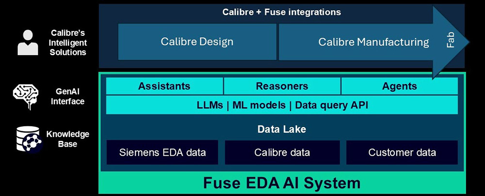
Trust comes when engineers can maintain full control and visibility, supported by intelligent automation that explains its reasoning. Collaboration becomes easier when tools let teams share debug context, assign issues and align on resolutions. This preserves institutional knowledge and keeps teams moving forward efficiently as complexity scales.
AI should empower engineers, never replacing their insight or making critical flows hard to understand. The combination of deterministic engines with actionable, explainable AI enables both speed and certainty in sign-off.
Transparancy
The stakes rise even higher when preparing chips for manufacturing, where yield optimization directly impacts production economics. Here, AI must be fast but also defensible to foundry partners and auditable when issues arise.
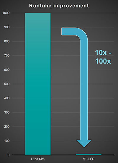
Machine learning algorithms can achieve 10x to 100x runtime improvements in lithographic simulation while maintaining the accuracy that advanced process nodes demand. The benefit is speed, but these tools must also provide the transparency needed for an engineer to act.
This means evaluating AI tools based on transparency of context as well as performance. Can the system quantify how strongly a violation belongs to a specific signal? Can engineers trace these patterns back to the physical layout and verification context? These capabilities transform AI from a productivity tool into a strategic asset for managing manufacturing risk and accelerating process ramp.
Deploying AI-driven chip design software across the design-to-manufacturing flow requires robust data governance, IP protection and engineer-in-the-loop workflows. Effective AI platforms address these through architectures designed specifically for semiconductor workflows.
Key principles include data sovereignty, where customers maintain complete control over their institutional data and when AI models are used. Transparency by design means AI systems provide the context for their recommendations, allowing engineers to audit decisions and override them when domain knowledge suggests a different approach.
For organizations in regulated industries – automotive, aerospace, medical devices – this governance architecture is the foundation that makes AI deployment possible while meeting compliance requirements for traceability and auditability.
The strategic value of transparent, governable AI extends beyond individual tool performance to organizational capabilities. When engineering teams can trust AI-surfaced patterns, they make faster decisions with greater confidence. When AI systems operate with clear context, they preserve institutional knowledge rather than creating opaque dependencies.
Design teams reduce verification cycles from weeks to days when AI helps them navigate billions of violations efficiently – but only when they trust the results. Transparent AI that connects design decisions to manufacturing outcomes helps teams catch yield-limiting patterns before tapeout, reducing costly mask revisions and production delays.
These benefits compound over time. Organizations that deploy trustworthy AI build confidence through successful outcomes, enabling broader adoption and greater impact.
Profound impact
The semiconductor industry stands at an inflection point. AI capabilities are advancing rapidly, but the real constraint isn’t algorithmic sophistication – the tools themselves are developing apace. The limiting factor is trust. Chipmakers need to trust the AI platform, the data security and the results.
In the near term, AI will mature as a focused tool for high-value tasks like power analysis, thermal prediction and yield forecasting. The industry is moving toward real standards for transparency and auditability, and customers will demand defensible, provable results.
Looking further ahead, AI will become a predictive engine for the entire design lifecycle. This vision requires an interconnected intelligence layer running across the whole flow, where general reasoning is continuously validated by deterministic verification engines.
The business impact is profound. Design teams will compress schedules from months to weeks, reduce respins and make data-driven calls balancing performance, power and cost. Manufacturers will see yield gains through earlier intervention and continuous learning on the fab floor.
For semiconductor companies, the strategic question isn’t whether to adopt AI, but how to deploy it in ways that amplify engineering judgment rather than replace it. The answer lies in systems that combine deterministic precision with interpretable intelligence, wrapped in governance frameworks that preserve control and visibility.
The semiconductor industry has always been built on precision and reliability. The future belongs to teams that can move fast with confidence. That requires AI-driven chip design software systems built on a foundation of trust.