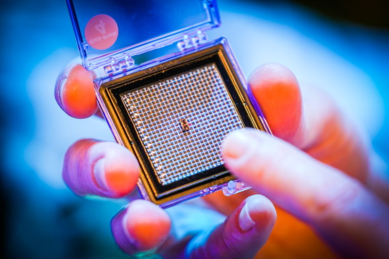
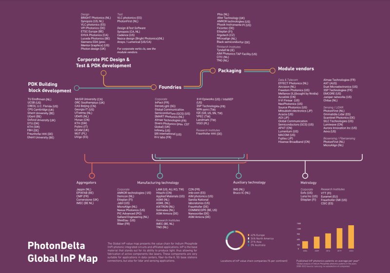
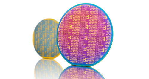
No technology platform can do it all in integrated photonics. In part II of a four-part series, we take a closer look at a base material that stands out for its ability to produce light, thus allowing for the fabrication of active components: indium phosphide.
Indium phosphide (InP) is a remarkably versatile material. Electronic circuits based on this compound semiconductor are among the fastest available today, operating at frequencies well beyond 100 gigahertz (for comparison, modern PC and laptop processors typically clock at 3-4 gigahertz). In photovoltaics, InP – mixed and stacked with various other III-V compounds – is an essential ingredient of ultra-high efficiency solar cells, used in space applications or concentrated solar power systems on Earth.
By far the most prominent use of InP, however, is found in optoelectronics. InP lasers produce light for optical communication systems all around the world, ranging from optical fiber connections and networks to free-space optical communication. Streaming companies, mobile communication operators and smartphone manufacturers all owe a debt to InP.
In recent years, InP has started to take on more responsibilities beyond merely producing light. Decades-long research efforts spearheaded by Eindhoven University of Technology have paved the way to build full-fledged light-based integrated circuits on InP substrates. Initially primarily for use in communication technologies, but by now, they’re also being targeted for sensor and imaging applications in automotive, healthcare and other markets.

Efforts to commercialize these research results are well on their way. “InP chips constitute a two billion dollar a year market already, which is growing rapidly,” says Johan Feenstra, CEO of Smart Photonics, the world’s first pure-play InP integrated-photonics foundry, based in Eindhoven, the Netherlands. “About half of those sales are relatively simple laser chips, the other half concerns the more complex devices that my company focuses on. Over the past few years, we’ve seen a strong growth of interest in our services. I’m convinced that trend will continue. InP technology is definitely leaving behind its status of being a promising technology and is showing viability in commercial environments.”
“As multiple markets have started to adopt integrated photonic circuits based on InP, the commercial prospects of this technology are definitely promising,” agrees Belinda ten Geuzendam, market research analyst at Photondelta, the Dutch end-to-end value chain for photonic chips. “For example, the market for 100+ gigahertz optical transceivers is predicted to grow at a rate of 20 percent per year over the next few years.”
“Another example is the lidar market,” Ten Geuzendam continues. “These systems using visible and near infrared light for detecting and identifying moving objects are an important technology for self-driving cars. This market is expected to take off in the coming years. As many as one in four cars sold in 2030 could be equipped with such lidar systems.”
Moore’s Law
InP has the longest history of all three major integrated-photonics platforms, which also include silicon and silicon nitride. There’s a good reason for that: if you want to build the light-based equivalent of an electronic circuit, you’re going to need a material that’s not only capable of ‘conducting’ light but also of being able to produce it, which translates into the ability of also making active (in addition to passive) components. As a so-called direct band gap semiconductor, InP is the only material that ticks both boxes, whereas the two silicon varieties do not (see inset “Why InP is a good light source, and silicon isn’t”).
There are many direct band gap semiconductors available, and in principle, these could all be used to fabricate integrated photonics. InP became the trailblazer of this technology because of historic reasons, Feenstra argues. “It was already being used in optical communications technologies based on discrete components. For reasons of backward compatibility, it makes sense to keep using the same wavelength ranges when integrating components, and therefore to stick with the same base material. However, if the integrated-photonics industry could pick any material it wants, without any historical considerations, it would still pick InP. It has all the required characteristics.”
After the invention of the semiconductor laser – essentially, the ‘transistor of integrated photonics’ – in 1969, the first photonic integrated circuit consisting of a laser and a modulator was reported in 1987. It was partially based on InP. From then on, the number of components integrated on a single InP chip grew exponentially, much like Moore’s Law in electronics. By now, photonic integrated circuits (PICs) with over a thousand components are manufactured in research environments. In Feenstra’s foundry, hundreds of components per chip are feasible.
The component density will continue to increase for at least another two decades, TU Eindhoven InP pioneer and one of Photondelta’s ‘founding fathers’ Meint Smit and colleagues wrote in 2019, though the researchers “do not foresee integration levels as presently achieved in digital microelectronics: physical dimensions and heat dissipation of photonic circuits are orders of magnitude larger than those of transistors.” In that respect, photonics resembles analog and RF electronics, which also feature much lower densities than in state-of-the-art CMOS.

Demand curve
Meanwhile, as previously mentioned, InP technology has started its trajectory of commercial maturation. In communication technology, it’s only a matter of time before InP PICs will be applied in data centers, fiber-to-the-X (where X is a home or any other type of building), connections to 5G base stations and many other places. After all, with the world’s appetite for bandwidth ever increasing, it’s hard to pass on the ability to increase data rates by sending signals in parallel using different wavelengths (called multiplexing) as well as by manipulating the phase, amplitude and polarization – all while using less energy than the equivalent electronic systems would need.
One prominent contender in the optical communications domain is Effect Photonics, the Eindhoven-based developer of InP-based optical transceivers and one of Photondelta’s champions. Founded in 2014, the Dutch company has recently been rapidly transforming into a revenue-driven manufacturing firm that operates internationally. Effect Photonics is a customer of Smart Photonics.
InP integrated photonics may have been originally developed with communication technology in mind, Feenstra has observed that the technology is increasingly finding traction in sensor applications these days. “Fiber-optic communication typically utilizes bands centered around 1,550 nanometers and, for shorter distances, the 1,310-nanometer bands, both of which are within the scope of InP. This near-infrared light can be used for sensors as well, ranging from automotive lidar to health and environmental monitoring. These are potentially very high-volume markets as well, just like the communications market.”

Examples of sensor companies using InP-based integrated photonics include Photonfirst from Alkmaar (fiber-optic sensing of temperature, pressure or deformation changes for a wide range of markets), Scantinel Photonics from Ulm, Germany (automotive lidar) and Mantispectra from Eindhoven (portable spectrometer for agrifood applications).
To accommodate the expected rise in demand for InP wafers, Smart Photonics has recently expanded its capacity from 500 to 5,000 wafers per year. “In addition to growing this capacity, we can upgrade the line from 3 to 4-inch wafers as well to double the output. The next step would be to build an entirely new facility capable of handling high volumes.”
The timetable of the stepwise capacity expansion isn’t set in stone. “There are two separate drivers at work. InP chips are traditionally made by the same companies that use them to manufacture communications equipment. By vertically integrated companies, in other words. Just like in the electronics industry, they may want to outsource production to foundries once they consider that to be a viable option. Companies developing sensor and other applications, on the other hand, will need to rely on foundries from the start. So, their demand curve is primarily a matter of technology and market development.”
This article was written in close collaboration with Photondelta.


