Swedish startup Alixlabs is preparing for manufacturing and commercial deployment of a new semiconductor patterning technique that unlocks leading-edge semiconductor manufacturing without the need for EUV lithography. The European Chip Desert should take advantage, says co-founder Jonas Sundqvist.
In 2015, around Christmas time, researchers from Sweden’s Lund University got an unexpected result. Having attempted to decrease the diameter of nanowires placed horizontally on a surface, the structures hadn’t only shrunk, they had also split in two. For every nanowire, there were now two thinner ones. In other words, the researchers had created a finer-pitch pattern without using lithography.
It didn’t take long for lead researcher Jonas Sundqvist to realize that this was something special. With plenty of experience in the semiconductor industry on his CV, Sundqvist was well aware of the importance of double patterning. At the time, it was effectively chipmakers’ only option to continue CMOS scaling while EUV lithography was still being industrialized. “I couldn’t stop thinking about it,” says Sundqvist.
Four years after the unexpected Christmas gift, Sundqvist and his colleague Dmitry Suyatin were confident they would be able to offer the semiconductor industry a new multi-patterning option, one with fewer process steps and therefore significant cost savings. They started Alixlabs in 2019, headquartered in Lund, together with co-founders Amin Karimi and Stefan Svedberg.
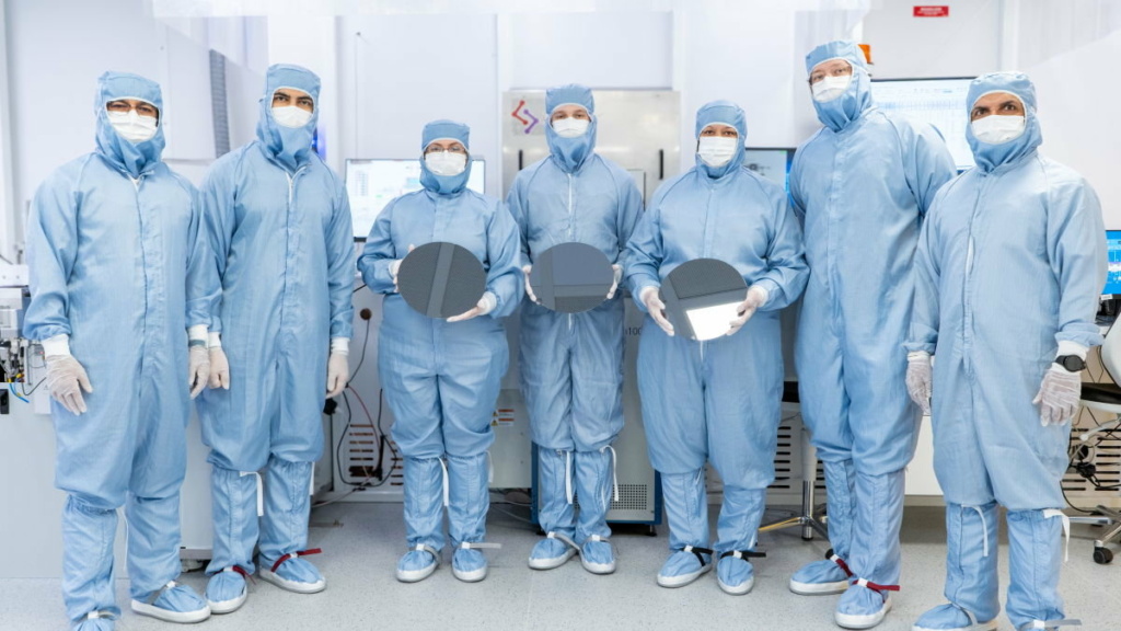
Working with Intel, the startup recently demonstrated 12.5nm half-pitch fin structures in bulk silicon without the use of EUV. These dimensions are found in today’s 3nm-class leading-edge logic. “Our mission is to create equipment that allows companies that don’t have access to EUV tools to scale down their production to 5nm and beyond. By eliminating the dependency on EUV lithography, we’re offering the industry a path toward more sustainable and economically feasible high-density chip production,” states Sundqvist.
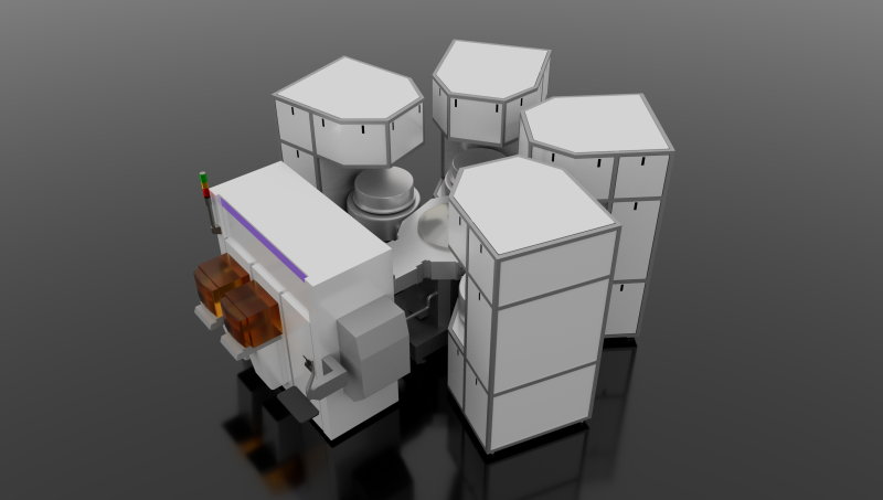
Alixlabs has joined hands with the Dutch semicon supply chain to construct beta tools, which are intended to bridge the gap between lab demonstration and full commercial deployment. Dutch deep-tech fund Forward.one is one of Alixlabs’ prime investors. “The Netherlands is kind of a one-stop shop for us,” Sundqvist quips.
Competitiveness
The core technology underlying Alixlabs is atomic layer etching (ALE), a cousin of the much more mature atomic layer deposition (ALD) technique. Where ALD adds a single atomic layer in a self-limiting process, ALE removes one. First, the top layer of a substrate is modified using a reactant gas. Afterward, a second reactant (or ion bombardment) is used to remove the modified material. Compared to other etching techniques, key benefits of ALE include its gentle nature, precise control of etching depth, high selectivity and 3D shape fidelity.
In a technique named atomic layer etching pitch splitting (APS), Alixlabs applies a sequence of traditional etching steps and ALE to double or even quadruple the density of a line pattern. Conceptually, this is similar to self-aligned double (SADP) and quadruple patterning (SAQP), which, even after the advent of EUV, are still applied in semiconductor manufacturing. Unlike APS, however, SADP and SADQ require a combination of multiple deposition, etch and cleaning steps along with advanced process control and metrology. This drives up capital and operational expenditure and fab cycle times, reduces throughput and introduces risks of defects. In terms of cost per good die, APS therefore compares favorably with the established multi-patterning techniques, says Alixlabs.
The cost of chip manufacturing escalates dramatically as node sizes shrink, with wafer prices jumping from a few thousand dollars at 65–28 nm to tens of thousands at 5nm and below. This is driven primarily by the extreme complexity of advanced nodes: once processes reach 7nm or smaller, chipmakers must rely on costly EUV lithography combined with multiple patterning, which lengthens process flows, raises capital intensity and increases defect risks. Furthermore, the industry faces a shortage of highly skilled laborers, resulting in bottlenecks that hinder capacity scaling.
Although APS is by definition complementary to lithography, its ability to densify chip features also positions it as a competing technique. Lithography is by far the most expensive component in running a fab, especially in the EUV era. “For some chip layers, APS will be an attractive alternative to lithography, for others not at all. Lithography and APS will co-exist as chipmakers optimize for cost,” says Fred Roozeboom, advisory board member at Alixlabs and an expert in ALE and ALD. “We estimate that APS has the potential to reduce leading-edge logic and memory wafer manufacturing costs by up to 40 percent per mask layer, while simultaneously increasing throughput,” Sundqvist adds.
Another consideration that factors into chipmakers’ choice of preferred patterning technique is sustainability. Advanced fabs also demand large volumes of critical minerals, land, clean water and energy, compounding both financial and environmental costs. Additionally, high CO2 equivalent emissions from these intensive processes run counter to global net-zero goals, putting pressure on manufacturers to balance competitiveness with sustainability.
“By reducing EUV use and the number of process steps, and therefore cutting energy and materials use, APS will both boost chipmakers’ competitiveness and drive sustainability goals,” says Sundqvist. His firm targets adoption of APS technology by the world’s top foundries for 2nm processes.
Take the plunge
For Europe, Sundqvist and Roozeboom argue, APS may be the best hope of rekindling local leading-edge semiconductor manufacturing. “I call APS the poor man’s solution to leading-edge manufacturing. After all, with relatively modest lithographic means and the power of APS, you can manufacture leading-edge nodes. The Chinese leverage multi-patterning techniques to manufacture 7nm chips and, depending on how much trust you put into internet rumors, 5nm chips as well. With APS, you can go even more advanced,” Sundqvist points out.
“It’s strange, when you think about it. With ASML, ASM and Imec, it’s Europe that controls scaling. Yet, further down the leading-edge supply chain, Europe is nowhere to be found. We’re stuck at 12nm, which will be the most advanced process ESMC in Dresden will be able to run. In the age of AI, this is unacceptable,” Roozeboom maintains.
Sundqvist: “I strongly believe ‘newcomers’ like Europe can penetrate the leading-edge arena with a litho-light approach to patterning. Why wouldn’t that be the case? TSMC, Intel and Samsung continued to be very successful in the multi-patterning era. Thanks to APS, the upfront investment required to build a leading-edge facility decreases dramatically, making it much more feasible than it used to be.”
Whether Europe takes the plunge or not, the Alixlabs CEO expects his tools will prove quite popular with Asian customers. “I’ll happily take orders from China like all the other tier-1 OEMs. It’ll be up to the EU and the Swedish government whether I’m allowed to ship them. If I’m not, I expect it’s made up to me in other ways. Like that European fab I was talking about.”
This article was written in close collaboration with Alixlabs. Top image credit: Alixlabs