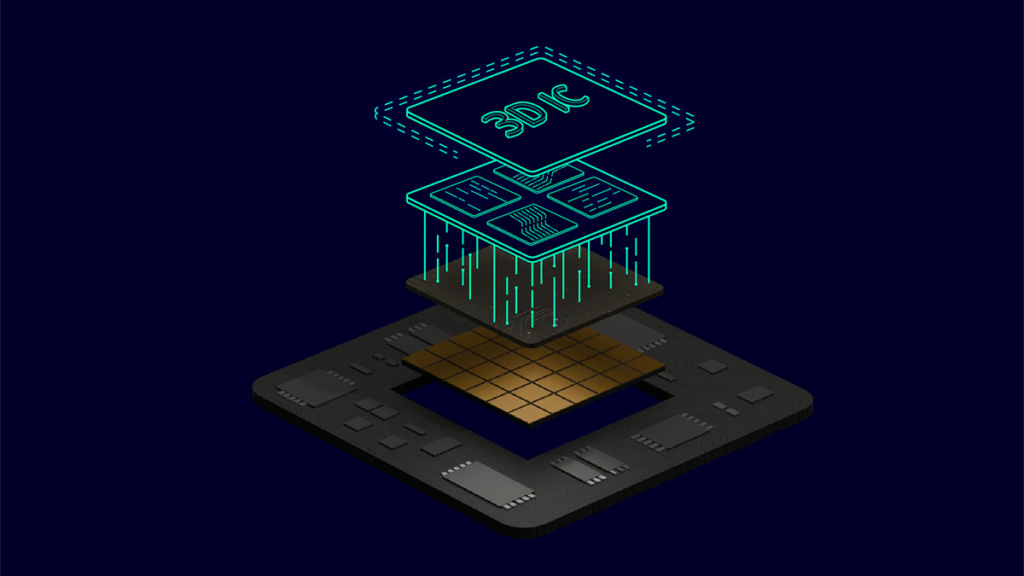
3D IC development introduces new system-level hurdles that demand innovative solutions that address exploration, design, analysis, reliability and test.
The semiconductor industry is at a pivotal moment, truly an inflection point where the very fabric of computing is being redefined. As the relentless march of AI propels us beyond the traditional confines of Moore’s Law, the familiar landscape of 2D SoC design is encountering its inherent limitations. The path forward, the very future of chip innovation, is now undeniably paved with 3D.
3D ICs integrate hundreds of chiplets and millions of interconnects within a single package. At this density, thermal, warpage and other multiphysics effects can cascade across the stack, causing costly re-spins and delayed time-to-market. These 3D architectures introduce entirely new system-level hurdles that demand innovative solutions to achieve the performance and reliability we’ve come to expect.
Collaborative work
A new methodology named system technology co-optimization (STCO) is extending the boundaries of design scaling. STCO enables architectural and technology trade-offs early in the system design process to achieve high-performance, cost-effective solutions in a reduced timeframe. Predictive analysis is a fundamental component of STCO that leverages high-level modeling and analysis during the planning phase.
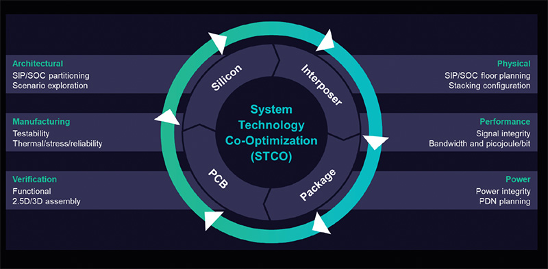
To determine which microarchitecture best meets a product’s requirements and objectives, high-level predictive analysis assesses a multitude of different chiplet-level SoC decompositions. The system or RTL design architect typically performs this analysis, but it also considers packaging technologies, available chiplet IP and off-the-shelf chiplet components. These considerations drive the need for collaboration between the system, RTL, package, ASIC and test teams early in the system design planning process – before the detailed implementation process begins.
As engineering teams integrate hundreds of chiplets and millions of interconnects into a single package, intertwined multiphysics and reliability risks grow exponentially. Heterogeneous integration combines separately manufactured components – chiplets, memory, co-packaged optics and sensors – into a single package using technologies like 2.5D/3D stacking, through-silicon vias (TSV) and interposers to improve performance, power, area and cost. An implementation 3D IC design flow requires collaborative co-design, including system-level partitioning, die-to-die interconnection planning, thermal management and comprehensive 3D system-level verification.
Heterogeneous integration in 2.5D and 3D IC development requires system-level electrical analysis that spans silicon, interposers/bridge and advanced packaging substrate materials. Traditional point-tool flows create silos, requiring manual net extraction, repeated data translation and late-stage debugging. As 3D ICs incorporate TSVs, micro bumps, hybrid bonding, fine-pitch redistribution layers and complex organic substrates, designers face many challenges. A unified flow that supports both early-stage and sign-off-quality system analysis is essential to reducing risk and accelerating tape-out.
Thermal and thermo-mechanical analysis and verification should start early and should be conducted continuously throughout all stages of design to prevent poor architectural and design choices. This is hindered by the fact that mechanical reliability modeling is traditionally done in siloed teams, often after the die and package design are completed. For advanced packaging, this must be collaborative work.
Model translation from electrical-to-thermal to thermo-mechanical is a key challenge and requires strong domain expertise. An integrated digital thread is required to improve the connection between package architects and thermal-mechanical analysts. Ideally, architects need the capability to initiate, trigger and carry out multiphysics simulations on their own to aid their design choices. The same models can be used as a communication vessel among teams, instead of Powerpoint, Visio or email descriptions.
In 3D IC packages, the concurrent execution of high-switching test patterns across several chiplets can cause excessive, instantaneous dynamic power, leading to thermal hotspots, overheating or device damage. Traditional structural test routines operate at the die level, lacking the package-level coordination to detect or prevent “red-hot” exposures during stacked die testing. This increases the risk of reliability degradation, silicon failure, reduced test yield and hard-to-catch thermal violations at the manufacturing stage.
Critical domains
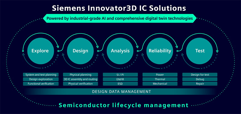
A unified flow, as provided by Siemens’ Innovator3D IC solutions, tackles the complexity of 3D IC design at every level. It proficiently addresses five critical development domains: exploration, design, analysis, reliability and test. Powered by industrial-grade AI and comprehensive digital-twin technologies, engineering teams can move faster, collaborate more closely throughout the entire lifecycle and deliver breakthrough performance for next-generation systems.