TSMC has committed to introducing ASML’s high-NA EUV lithography into high-volume manufacturing starting in 2030, marking a major shift for the world’s largest foundry after years of publicly downplaying the technology’s near-term value. The announcement came as part of a joint initiative with ASML to prepare the industry for a transition from today’s 6-inch EUV photomasks to 12-inch masks. With the introduction of the larger high-NA mask size targeted for 2033, however, TSMC will initially use the currently available masks.
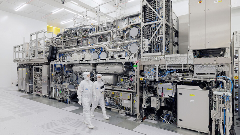
The commitment is significant because TSMC has consistently argued that in upcoming years, conventional EUV scanners will remain more cost-effective than high-NA. Although the Taiwanese firm acknowledged that it “would eventually use it,” the uncertainty about the timing made some ASML investors nervous. TSMC’s endorsement removes these doubts.
During the latest roadmap update presented earlier this year, TSMC said it had no plans to use high-NA tools for the A13 and A12 nodes, which are scheduled for mass production in 2029. It’s not clear which node or nodes will mark the debut of high-NA at TSMC.
TSMC’s commitment follows that of Samsung, which is also introducing high-NA in 2030. Intel has already started small-scale high-NA production and has confirmed deployment for the 14A node, slated to reach high-volume manufacturing in 2028.