Nokia has agreed to acquire NXP Semiconductors’ fab in Chandler, Arizona, intending to convert the RF GaN facility to manufacture InP optical components. The telecom company will begin leasing part of the fab in early 2027 before completing the acquisition in the first quarter of 2029, subject to regulatory approval.
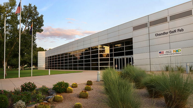
Heralded as “the world’s most advanced” fab of its kind at the opening in 2020, NXP’s Echo facility took up gallium nitride as a successor to LDMOS technology used widely in 4G. But falling operator investment and shrinking 5G rollouts hit the segment hard. NXP announced its exit from the market last December.
In 2025, Nokia acquired California-based Infinera, a vertically integrated supplier of InP-based optical components. That transaction included an InP wafer fab in San Jose and a packaging and test facility in Pennsylvania. Through the acquisition of the Chandler fab, Nokia is further expanding InP production capacity.
InP-based integrated photonics has garnered significant interest lately because of its key role in high-speed optical links used in the build-out of AI infrastructure.