
The world’s leading DRAM manufacturers are taking different approaches to the next generation of memory technology.
As conventional DRAM scaling becomes increasingly difficult, memory makers are plotting different paths into the future. Samsung and SK Hynix hold on to the so-called 4F² architecture as a worthwhile stepping stone to 3D DRAM, while Micron has decided to skip the technology, arguing that its manufacturing complexity outweighs the benefits.
A conventional DRAM cell consists of one transistor and one capacitor, horizontally arranged on the substrate. The transistor controls access to the capacitor, which stores information as an electrical charge. For decades, manufacturers have increased memory density primarily by shrinking the dimensions of these components and packing them closer together.
The physical area a single bit of data occupies on a silicon die is referred to as the memory cell size and is usually described in terms of F², where F represents a characteristic minimum feature dimension of the manufacturing process. Today’s mainstream DRAM cells occupy approximately 6F², typically arranged as a rectangle measuring 2F by 3F. Reducing that footprint to 4F², or 2F by 2F, would theoretically allow 50 percent more cells in the same area, assuming the same F.
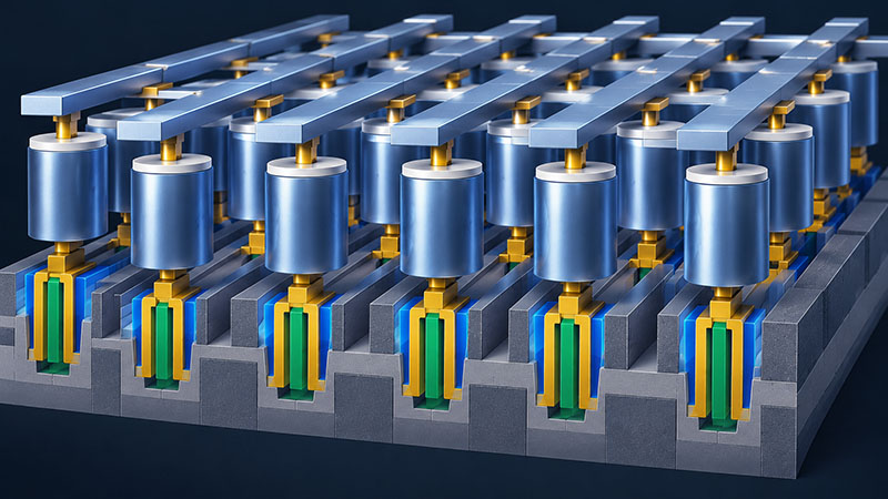
Achieving this reduction requires a substantial redesign of the access transistor. Rather than arranging its source, channel and drain laterally, manufacturers can stack them vertically, reducing the transistor’s footprint on the silicon surface. Samsung calls its implementation a vertical channel transistor (VCT), while SK Hynix is developing a vertical gate (VG) architecture.
Myth
The concept is straightforward, but implementing it is difficult. Vertical transistors introduce new challenges in controlling leakage currents, electrical characteristics and manufacturing variability. One particularly troublesome phenomenon is the floating-body effect, in which unwanted charge accumulation affects transistor behavior. These problems become increasingly difficult to manage as the dimensions shrink.
Moreover, a physically smaller memory cell doesn’t automatically translate into cheaper memory. The additional process steps, materials and manufacturing complexity required to produce vertical transistors may offset the density advantage. Ultimately, manufacturers must deliver more usable memory bits per wafer at a competitive cost.
According to Micron, which invented the concept and spent twenty years researching it, 4F² isn’t going to deliver. “It’s a bit of a myth that 4F² provides anything versus 6F². It’s the capacitor pitch that defines the DRAM. You can build the cells, the transistors in different ways, but they still have to fit under the capacitor pitch, which sets the DRAM. So, some of that is just kind of smoke and mirrors in terms of talking about 4F² versus 6F²,” the firm’s CTO Scott DeBoer said during a technology webinar in October.
Horizontal
By contrast, Micron’s Korean competitors are keeping 4F² on their roadmap. At the International Solid-State Circuits Conference (ISSCC) in February 2026, Samsung presented a 16 Gb memory chip combining vertical channel transistors with wafer-to-wafer hybrid bonding. The latter technology enables separately manufactured structures to be joined with extremely fine electrical connections, providing greater freedom in the arrangement of memory components.
According to industry reports, Samsung subsequently manufactured working dies using its 10a-generation process technology. The reported roadmap calls for development to be completed in 2026, followed by qualification in 2027 and mass production in 2028. However, Samsung hasn’t publicly committed to any schedule. At the SEDEX 2026 exhibition in October, CTO Song Jae-hyuk only confirmed that development was still underway.
SK Hynix is pursuing a similar strategy. “We’re preparing a step-by-step roadmap covering the extreme scaling of the existing DRAM to 4F² and 3D DRAM. Each technology will be applied to the right product at the right time, meaning when it’s ready technologically and economically,” an executive said during a recent earnings call with analysts.
For both Korean manufacturers, 4F² is more than another incremental improvement in cell density. Vertical transistors could also provide a technological foundation for eventually stacking memory cells in multiple layers. Such 3D DRAM architectures would allow manufacturers to increase density without relying exclusively on further reductions in lateral dimensions.
As the move from planar NAND flash to 3D NAND demonstrated, however, aggressive lateral scaling ceased to be the primary driver of density improvements. Stacking layers of more traditional horizontal arrangements of transistors and capacitors could be the best way forward in terms of performance, power efficiency and manufacturing yields.