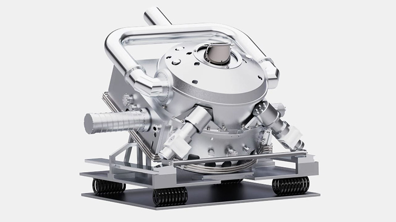
A researcher at the Okinawa Institute of Science and Technology (OIST) has proposed a new optical architecture for high-NA EUV lithography. The approach replaces today’s highly complex optical layouts with a simpler in-line configuration that uses carefully arranged mirror pairs to maintain image quality at high numerical apertures.
The setup could significantly reduce the complexity and cost of next-generation chip manufacturing, says OIST researcher Tsumoru Shintake. “Current EUV lithography systems cost hundreds of millions of euros per machine. My new design should achieve fine, 2-3 nm scale details, in a much cheaper way compared to today’s state-of-the-art machines.”
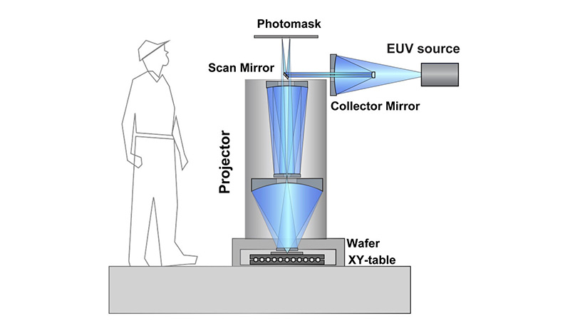
However, just as with Shintake’s previous work on low-NA EUV, ASML and Zeiss have evaluated similar designs, some even with better performance, an ASML spokesperson told Bits&Chips. “These designs haven’t generated chipmakers’ interest due to the reduced resolution and/or smaller field size of the design,” he said.
Any design for the EUV optics in a lithography tool is a trade-off between several factors. For bulk semiconductor manufacturing, image quality and throughput are key, and it’s safe to assume that ASML and Zeiss have optimized their high-NA scanner for that purpose. There may be a market for lower-cost, lower-throughput tools for smaller production runs, however.